Constraint Management—Rules-based design and verification to reduce design cycle time
By Ed Clark, business development manager, EMA Design Automation Inc.
Engineering Software Supply Chain design Design EDA EDA engineering engineering software softwareIn a time where deadlines are shortening and designs are becoming more complex, there is no room for error. Specifying rules and requirements upfront in the design process is one way to try and mitigate any future issues—even the simplest of designs have hundreds of rules which need to be managed. In many PCB design tools, these rules and requirements become constraints that guide the process to ensure they are all followed.
Along with increased design complexity, constraint complexity is growing. Most designers are already looking at rules regarding spacing allowances, dynamic phase tolerance requirements, propagation delays, return paths, etc., but as the number of constraints increases, so does the difficulty to manage them. For example, since differential pair constraints are set in both the physical and electrical domain, if you count all those rules plus any possible delay and match-delay rules, each differential pair can have as many as 13 specific constraints assigned to it. Multiply this by the number of differential pairs in the average design and you can see how overwhelming and difficult it can be to manage and maintain these constraints over time.
Why a Constraint-Driven Design Process?
The manual processes of communicating and maintaining constraint rules and requirements through ‘engineering notes,’ excel spreadsheets, properties, etc. will no longer suffice and can lead to miscommunicated constraints. This results in errors, causing unnecessary iterations between electrical engineers and layout designers. This process can then snowball the problem, eventually turning into a costly redesign or, at the very least, a lengthy project delay with additional costs. Nowadays, the key to success is to prevent any foreseeable design issues from occurring and to eliminate any other unnecessary design respins. Adopting a constraint-driven, aka correct-by-design (CBD), process can help do this.
CBD is a simple concept: it states that design rules (physical, spacing, electrical, signal/power integrity, manufacturing, assembly, and fabrication) need to be taken into consideration as early in the design process as possible to ensure the engineering design intent is implemented in the PCB design practices. Its main goal is to help identify and fix rule violations when they happen, not after numerous design decisions have been made based on faulty assumptions. With a constraint-driven process, intelligence is added early in the design phase identifying errors as they happen to guide the process past the pitfalls that can result in a respin.
While setting up and implementing this type of design flow may seem like a daunting task, this single point-of-truth for constraint and process management has been production-proven to shorten design cycle time. In fact, a recent Aberdeen study states companies who implement constraint-driven design more often experience first-turn design success, since it allows designers to identify issues before designs are pushed into production. These companies had 54% better performance on meeting product launch date targets.
In our competitive market, a constraint-driven design approach is no longer optional—it is a requirement for success.
Completing a design using double data rate (DDR) or high-speed designs would be impossible without a robust, constraint management system. In addition, the ability to tune nets directly from the feedback of this system while routing or using an autorouter to follow rules is imperative. Cross-probing, the ability to mark errors to be fixed or waived, or the ability to tell if the error is okay from an engineering, assembly, or manufacturing perspective is not only critical, but a requirement. Often, chip and board vendors will supply topologies and rules in ECAD formats, but if the design dictates a change in the form factor, the designer will need to do constraint development himself.
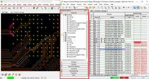
Figure 1: The constraint manager keeps everything organized, very efficient and easy-to-use.
In figure 1, the tabs on the left side of a constraint manager (the highlighted red rectangle) shows the “Electrical” tab is open. Notice how everything is organized, very efficient, and easy-to-use. This makes the difficult process of managing the complexity simple and is the key to productivity and first-spin design success.
To the right of the electrical tab is a spreadsheet of the constraints. It shows some of the DDR3 constraints required for this design and defines each constraint. In this case, it shows a matched group of signals (Bank0) that had to be length-matched (it could also be defined in time—pS) to strobe line within 25 mils. The red highlighted text fields on the right side shows two columns: Actual (routed length) and the Margin (of error). The values are shown in red because the traces have not met their respective constraints.
Intelligent Constraint Development and Implementation
During the development process, to create the constraints needed to achieve a design with sound signal quality in addition to completing any other design requirements, you must be able to do a graphical constraint definition in the schematic or before the net is routed.
A unified and integrated approach to visualizing and simulating the circuits to create the proper impedances and matched delays (relative prop delays, lengths, and topologies) is of critical importance for the design to perform “correctly by design” such that the design intent and IP are maintained, implemented, and verified in real-time.
As the adage goes, Garbage in = Garbage out. In the design world, ‘garbage out’ equates to design respins. Therefore, it is critical to have the proper constraints in place as well as an advanced stackup editor which includes impedance calculators (single-sided and differential) that can easily be stored and reused in a single technology file. The accuracy associated with these impedance calculations can help ensure manufacturing accuracy and assures signal quality. Figure 2 shows the characterization of a digital signal going from one driver pin to two receiver pins. The simulation will show the effects of the series termination resistor, routed topology, length, and impedances of the segments. It is very important to note that all these elements can be swept over ranges of values to find the perfect solution space for this design’s intended application and mitigating other issues like electromagnetic interference (EMI). Simulation allows a designer to correctly constrain a net, like the one shown, without over constraining it.
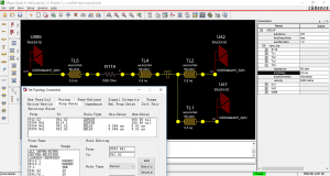
Figure 2: This shows the characterization of a digital signal going from one driver pint to two receiver pins.
It is also essential for a Constraint Management System (CMS) to be stackup aware. Since the PCB stackup plays a major part in the design process, repeatability and accuracy describing the PCB stackup with accurate representation of the materials and rules are essential to a CBD workflow.
Figure 3 shows both a tabular and graphical view of the layers on the board (the stackup). The materials, line-width, thickness, and spacing can be studied with the help of integrated field solvers for instantaneous feedback on single-ended impedance and differential impedance.
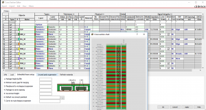
Figure 3 shows both a tabular and graphical view of the layers on the board (the stackup).
Every design will have design rule violations; however, depending on the design density, the number and types of design rule check (DRC) violations can quickly become overwhelming, requiring weeks to check each one (or take the risk of a fatal design flaw). What is critically important to manage is the spacing, physical and electrical rules, and violations (DRC Errors). These errors must be managed in such a way that the designer can easily cross-probe the issue and either fix or waive it in a managed way. Without a centralized, unified CMS this is nearly impossible. Figure 4 shows an example of how a good CMS can provide an overview of the constraints and highlight which ones still need work. DRC markers on the PCB layout provide a good feedback mechanism to the PCB designer and keeps them aware of problems as they arise. However, a single move of some copper can cause an avalanche of DRCs, making it difficult to see which to address first. The CMS provides a nice overview and allows cross-probing between the design and the constraint violations to easily pinpoint the problems.
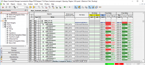
Figure 4
Developing a good set of constraints can take a fair amount of design time, but hopefully it is now clear that the follow-on time savings and error-avoidance far surpass the initial effort. In addition, a good CMS can provide one more big time and error saver: it can save and load constraints. All the effort you put into constraint development will continue to pay dividends in future designs. Obviously, all designs are different and will require their own level of constraint development, but there is also commonality. For example, if several designs have DDR3 busses in them, then reusing all that up-front work makes the next DDR3 design easier with pre-created, pre-vetted constraints.
What to Look for in a Constraint Management System
A sound constraint management design process makes correct-by-design a reality, reduces time-to-market, and ultimately optimizes the design process—eliminating the undefined, error-prone methods of the past. When looking for a constraint management system, be sure to ask yourself the follow questions:
-
Does the system understand engineering rules required for layout and manufacturing? Can it pull rules from multiple sources?
A robust CMS will be unified and integrated into the schematic and layout editors with cross-probing including:
- Integrated graphical topology-driven constraint definition, simulation, and application
- Length or time-based constraints
- Full suite of electrical constraints with custom formula capability
- Robust physical and spacing rules (class to class rules)
- Regions rules for spacing and physical constraints
- Same net DRCs for advanced technologies (HDI)
- Impedance rules (checking for nets crossing gaps in the planes or voids)
- Manufacturing rules
- Assembly rules
- Fabrication rules
- A robust stackup editor with board material and loss tangents
- Integrated field solvers and extraction
- Lossy frequency dependent transmission line pre/post route simulation and extractions
- Via modeling and extraction
-
Can the system easily communicate design intent amongst various team members?
Most constraints are known or discovered during the initial design creation—when the design is being captured in a schematic. It is therefore best to be able to define those constraints during the schematic phase. Then they need to be available during PCB layout, when most constraints are used. However, some constraints are determined during layout, so those need to be documented as well and made available to those working on the schematic. This back and forth communication of constraints is the key to a successful project, especially as team size grows.
-
Can the system check your design for errors and provide feedback in real-time?
The main idea behind setting constraints upfront is to help ensure the design is going to function as expected. Therefore, it is important that the system can alert the designer to any errors as they occur, so no progress is accidentally made based on bad design. Think of the constraints like the bumper cars at a carnival: sometimes the cars are hard to keep straight, but the bumpers on the car (the CMS) are there to help bring the car (the design) back on track quickly.
-
Is it flexible/easy-to-edit?
Who wants to replace one arduous task with another? Having a CMS that is flexible and easy to work with is essential to a successful implementation. Best CMS systems will allow designers to manage constraints directly within the CAD environment, allowing teams to get up and running quickly.
-
Are the embedded constraints and rules reusable amongst other designs?
While a team’s designs are not all the same, there might be some constraints or rules which can be applied to multiple designs (i.e., electrical rules). To save time and reduce errors, it is imperative that a CMS allows for the reuse of these assets.
Preparation Leads to Success
When constraints are done in the beginning of the design process, designers can be confident knowing once the design phase is done, it will move through the other phases with fewer or no errors requiring redesign. A CMS that can check work in real-time, as the design process is executed, provides reduced risks and the peace of mind that once board routing starts, the constraints will keep the board designer from violating any of the rules set up front. A constraint-driven, correct-by-design workflow helps to reduce respins and ultimately saves time and money. While we cannot always plan for the unexpected, setting the proper design foundations and having a reliable CMS will leave you prepared should an issue arise.