Henkel opens technical application centre
EP&T Magazine
Electronics Production / Materials Supply Chain materials productionSilicon Valley facility to foster next-generation electronics development
Henkel recently opened its new application centre in Santa Clara, CA designed to support product development for the company’s high-tech customers in the Silicon Valley region. Equipped as a state-of-the-art facility, the Application Center will help expedite proof-of-concept initiatives for electronics advances.
“The current pace of technology progress is unprecedented,” says Stefan de Diego, Henkel Regional Head of Electronics, Americas and Europe. “And, for today’s innovators, being first to market is integral to commercial success. With our knowledgeable team and extensive lab resources – located in the global epicenter of tech innovation – Henkel can provide even more immediate and impactful prototype design and analysis support for our customers, helping them meet critical time-to-market windows with tested, proven devices.”
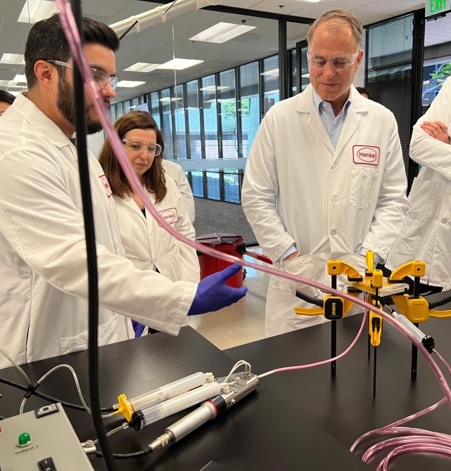
Jan-Dirk Auris (right), executive vice president, Henkel Adhesive Technologies, observes a colour-matched adhesives demonstration from application engineers Efren Jimenez (left) and Burcak Conley.
As a global leader in adhesives, sealants and functional coatings, Henkel has formulated thousands of materials that are vital to the form, function and reliability of the technologies powering modern-day life. Whether it’s 5G handheld devices and mobile networks, data center high-performance computing and optoelectronics, smart home systems, autonomous driving or virtual reality and gaming, Henkel materials and solutions enable robust electrical connections, heat management for optimized performance, protection from stress and environmental conditions and long-term durability. Henkel’s Santa Clara Application Center offers a true co-development environment, with access to all the resources required for technology design and testing.
The investment of about USD$2-million includes dispensing robots, 3D printers, mechanical property evaluation equipment, coating and jetting systems and failure analysis capabilities, among other assets. In addition to the hands-on laboratory, the facility provides multiple secure collaboration spaces for Henkel’s technical experts and its customers, as well as digital platforms for virtual engagement opportunities.