Boreas Technologies targets disruption of haptics sector
Stephen Law
Circuit Protection Electronics Production / Materials Engineering actuators actuators haptics haptics piezo drivers piezo drivers piezoelectric piezoelectricBromont Quebec-based firm set to strike in the haptics space, particularly after discovering there are limited manufacturers of drivers suitable for piezoelectric actuators in the global market
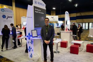
Boréas Technologies’ founder and CEO Simon Chaput stands at his firm’s booth during the CES Show in January.
After a long period of relative inactivity where haptics research was confined to a fairly tight group of companies and academics, the industry is about to be significantly disrupted and transformed by newer technology options. Leading the way is Boréas Technologies of Bromont Quebec, one of many new players to emerge by developing new advanced haptics solutions.
In this article, EP&T poses a few questions to Boréas Technologies’ founder and CEO Simon Chaput. He quickly recognized the opportunity to strike in the haptics space, particularly after he discovered there are limited manufacturers of drivers suitable for piezoelectric actuators in the global market.
Provide us with a brief overview to your education and how you uncovered these elements of design.
I did my undergraduate degree and master`s at Université de Sherbrooke in Québec. During my master`s, instead of pure academic research, I did an industrial research project with Teledyne DALSA in Bromont, QC. The objective of the project was to design a 3V to 300V boost converter to enable the use of MEMS micromirror in portable devices. Toward the end of my master’s, I wanted to do a few more years of research before jumping into the job market. That`s when I was accepted at Harvard University. While looking for a research topic at Harvard, I met with people from GE who were looking for a better piezo actuator driver for a cooling fan application. I decided to work on that problem and after reviewing the state of the art, I came up with a new piezo driver architecture that enables to create drivers that are at the same time low power, miniature, low cost and have very low output distortion. While the architecture was designed for a piezo fan at the beginning, these four attributes made the architecture perfect for haptic applications.
Outline your research and how you intend to disrupt the haptic driver market.
Piezoelectric actuators are well-known in the haptics industry and they are the actuator type offering the best haptics performance compared to other type of vibrotactile actuators such as Eccentric Rotating Mass (ERM) and Linear Resonant Actuator (LRA). However, piezo require a high voltage to achieve meaningful force or displacement. Depending on the specific actuator, this voltage can be anywhere between a few tens of Volts to multiple hundreds of Volts. While piezo actuators are extremely efficient at transforming electrical energy into mechanical energy, miniature electronics for piezo actuators is very inefficient at transforming a battery voltage (e.g. 3.6V) into the high voltage required. Consequently, piezo actuators for haptics never reached the mass market.
To promote its ultra-low power piezo drivers Boreas Technologies demonstrates a buttonless smartphone. This design replaces the mechanical volume and power buttons with two piezo actuators next to the frame.
Our CapDrive technology sets the new standard in terms of piezo drivers. First, it reduces power consumption by 10X compared to our leading competitor which not only reduce the energy requirement of a piezo haptic solution, but it also makes piezo the most energy efficient haptic technology on the market. Energy efficiency is a big thing for our battery powered devices. Second, it takes advantage of the unique ability of piezo actuators to act as a sensor and actuator. So far, on the market, you can find ICs that are able to sense or drive an actuator, but our CapDrive technology enables to do both which reduces significantly the size and cost of the system. Third, our first product has the smallest footprint which enables our customers to implement piezo haptic within a very small footprint.
We believe that by providing a piezo driver technology that is small, low-power and that has the capability of sensing, we will enable many systems to move from R&D to product.
Describe your SmartClik piezo actuator technology, unveiled at CES this January, as proof of concept for future buttonless smartphone designs.
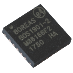
BOS1901 piezo driver is a single-chip piezo actuator driver with energy recovery, based on a patent pending CapDrive technology.
Our SmartClik technology unveiled at CES is embodied in a phone that has no traditional button. Instead, it is made of an aluminum frame with no holes. Where traditional buttons are, we placed piezo actuators inside the frame. Since our CapDrive technology can sense and drive, when the user press at the correct place on the frame, we detect the action and send a feedback that feels like a mechanical switch. While imitating the feeling of a mechanical switch is a very basic haptic effect, piezo buttons offer a wide range of advantage to phone OEMs. Like localized haptics, dust and waterproofness and different types of feedback from the same button depending on the application.
SmartClik is the first concept we did, but we plan to create other devices using our chip. The plan was to put into engineers hands a device that proves the concept. Haptics isn’t something you can easily understand with charts and spec sheets, you need to hold it and feel it to really understand the difference between crude vibrations and HD haptics.
A lot of people tried our SmartClik phone at CES and we still enjoy seeing the reaction on the user’s face when we unplug the phone and they understand that what they thought was a button was, in fact, a pretty stiff aluminum frame that doesn’t move.
Boréas aims to lower the bar for replacing physical buttons with virtual ones. How important will haptics become in the design of electronic devices of the future?
Haptics will become increasingly important in electronic devices because most form factors are either moving to a a customizable interface to increase the device functionality and improve the user interface (e.g. Lenovo Yoga notebook display keyboard) or they are removing buttons to achieve a more robust and aesthetic design (Vivo Apex 2019 phone).While physical buttons are easy to use, they are limited to a single function and they are often a weak point of the device. However, as a human, we don’t like to interact with a solid surface that doesn’t provide any kind of feedback when you press on it. Consequently, as computers, mobile devices, cars start to implement solid state interfaces to meet different functionality objectives, haptics will become more important to offer a satisfying experience to the user.
Which design application sectors do you anticipate being the most impacted by Boréas’ innovations in the haptic driver market?
It is hard to answer which sector will be most impacted as we see a lot of interest from mobile devices, laptop/tablets, wearables and automotive for our technology. However, we believe that the first sector to adopt our technology will be mobile devices.
Among its pending innovations, Boréas has developed high-definition haptics that imitate the texture of a sweater’s fabric so that people shopping on their devices can feel before they buy.
How close are you to making this a reality?
We didn’t develop this technology. We are using it as an example of what haptics will be in 5 to 10 years so that people understand easily the potential of haptics. There are already companies who have prototypes of texture-based haptics, however a common problem for these prototypes is the size of the electronics as well as the energy required. Boréas expertise in miniature low-power haptic drivers will enable these companies to reduce the size and cost of their solution as well as make their solution viable in a greater range of applications.

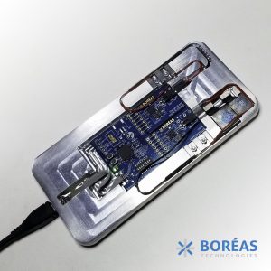
BOS1901 Development-Kit.
Boréas recently introduced its SmartClik technology, a proof of concept for future buttonless smartphone designs, using ultra-low-power haptic semiconductor technologies. How will this development evolve smartphone design?
This design helps OEMs manufacture more reliable devices. Mechanical buttons are subject to failure, create a breach in the device that can let water and dust get in and they have only one function.
Haptic buttons allow the device to be completely closed, improving the devices’ dust and waterproofness. Since they don’t move, they’re also less prone to failure. They can also be programmed to trigger different actions. For example, on our SmartClik phone we can program multi-level pressure sensing. You could control volume with one single button: a light press could decrease volume and a hard press could increase it. Open another application and this button could trigger the camera. You can program the button to do whatever you need with the phone software.
A couple of OEM are already moving that way, but with legacy haptic technologies (LRA). Those technologies make the whole device vibrate when you click on the haptic button, which doesn`t provide a realistic effect. Piezoelectric actuators have the advantage of giving a very localized feedback. Only the pressing finger will feel the button.
This design also helps engineers create better localized HD haptic feedback. By replacing buttons around the phone, you end up with piezoelectric actuators all around the frame. You can trigger localized feedback on the device depending on the application. This will enable OEMs and app developers to create a more engaging user experiences while using the same generic hardware that will be in all devices in the future.
While Boréas is not the only chip vendor working on piezoelectric-based HD haptic feedback, how do you stay ahead of the competition.
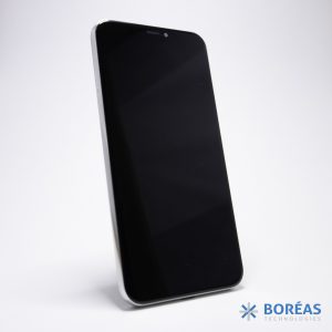
SmartClik Concept Phone
Like stated earlier, the main challenge for piezoelectric haptic technologies was power consumption. Other piezo drivers consume too much power because they’re based on miniaturized designs of audio amplifier architectures. They were not designed from the ground up with battery powered mobile devices constraints in mind.
With our patented CapDrive architecture we can drive the same piezo actuators but consuming up to 10X less power. This argument alone is a major differentiator over our competitors. We keep an eye on the market to be aware of new developments, but we haven’t seen something come close to our unique technology.
Have the developer kits, focused on piezoelectric actuators, generated interest from a wider designer community?
The response to our development kit has been very good. We sold many of them even if the kit was not available at any distributors. There are companies who did repeat purchase for different projects. While we are a small company, we already shipped kits to all our key markets: United States, Europe and Asia.
How important was it for you to keep Boréas in Quebec, versus being tempted to relocate to Silicon Valley?
People in the USA thought I was crazy to start a semiconductor company in Canada. Like I said earlier, I did my master project at Teledyne Dalsa, based in Bromont. There are a couple big companies specialized in electronics based in Bromont. I knew that I could easily find a highly qualified workforce there. After a few phone calls and meetings, my past colleagues from Teledyne Dalsa decided to join the company. Our team has an average of 20 years of experience. This allows us to move fast compared to traditional new semiconductor design teams. When I visit customers in Silicon Valley, they are impressed by our speed and quality of products.
On the financing side, development costs are also much lower in Québec than what it would have been in Silicon Valley. We developed our BOS1901 chip for a fraction of what it would have cost us in Silicon Valley. Our office is based in the C2MI building in Bromont. C2MI is a state-of-the-art collaborative R&D lab for microelectronic development where multiple companies, such as IBM and NXP, work on specific projects. Our location enabled us to rent all the specialized equipment we needed instead of buying it. Consequently, we were able to test our devices during development at our office instead of shipping our prototypes all over the world to subcontractors for testing. It allowed us to save money and significant time.
Plus, we have a nice mountain 5 minutes away from the office for outdoor activities like ski, mountain bike and hiking. 
Overall, our location enabled our company to access the skilled workforce needed and the development infrastructure required, reduce the company operating cost and provide a nice work-life balance to our employees. While it doesn`t have the hype of Silicon Valley, I firmly believe it is the best location for our company to grow into a major haptic semiconductor company.