Transparent conductive film set to alter design landscape
By Dr. Ragip Pala, Dr. Efthymios Kallos, Dr. Dong Han, Dr. Jonathan Waldern, Meta Materials Inc.
Electronics Production / Materials Engineering Supply Chain automotive design Editor Pick Electronics materials Meta-MaterialsInvisible, nano-structured metal mesh is fabricated onto glass or plastic surface
NANOWEB is an extremely thin, transparent, conductive film that consists of an invisible, nanostructured metal mesh fabricated onto a glass or plastic surface. With its transparency, conductivity and flexibility, the patented functional film holds good potential for both passive and powered use cases, with applications including electromagnetic interference shielding, antennas, 5G/6G redirection systems for elimination of dead spots and deicing/defogging devices for vehicle windows and eyewear.
NANOWEB technology
Transparent conductors are critical components in a wide range of electronic devices, including touchscreens, organic light-emitting diodes (OLEDs) and photovoltaics. They are also used in the optical components of sensors and display systems, including electromagnetic interference (EMI) shielding and transparent heating elements.
Existing transparent conductive electrode (TCE) materials, such as indium tin oxide (ITO) and silver nanowires, suffer from several drawbacks, including poor mechanical stability, low optical transmissivity, low electrical conductivity, high cost, and limited supply. These constraints (or limitations), together with the ever-growing demand for electronic products, have encouraged efforts to explore alternative solutions.
One outcome of such efforts is NANOWEB, a unique transparent thin-film conductor developed by Meta Materials Inc. (META).
Comprising a precisely arranged mesh of invisible submicron metal wires formed on a glass or plastic substrate, NANOWEB provides enhanced electrical and optical properties compared to conventional transparent conductor films. Distinct from currently available options, the material’s transparency is determined by its nanostructured wire mesh geometric spacing and submicron dimensions. As a result, it can be manufactured from almost any metal, including but not limited to silver, aluminum, nickel, copper and platinum, all to deliver expansive specifications and capabilities, while maintaining exceptional visibility.
In many cases, NANOWEB can function as a substitute for ITO, which is arguably the most commonly used TCE material. Furthermore, the material also outperforms ITO-based components in terms of sustainability and manufacturing energy consumption.
Another key advantage that differentiates NANOWEB from conventional solutions is its flexible mesh pattern design that can be customized and optimized to satisfy various application requirements. It is often impossible to cost-effectively pattern (etch) ITO much less than 20µm in thickness, whereas NANOWEB is printed from its roll-to-roll manufacturing line (not requiring any post-patterning etch step) with submicron features.
Rolling mask lithography
NANOWEB achieves its performance and versatility from its fabrication process called Rolling Mask Lithography (RML), which may be best described as a proprietary continuous near-field optical nanolithography process. Combining the benefits of phase-shift and soft lithography with roll-to-roll patterning,2,3,4 RML provides the capability to produce subwavelength structures for large-area applications in a cost-effective, scalable fashion. Through the use of a cylindrical elastomeric mask, a wide selection of materials (e.g., silver, gold, and copper) can be fabricated on both rigid (e.g., glass and sapphire) and flexible (e.g., plastic and flexible glass) substrates.
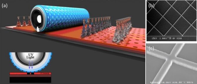
Figure 1a illustrates the RML technique for continuous nanopatterning over a large area and the main system components. Figure 1(b) and (c) show scanning electron microscopy (SEM) images of a NANOWEB pattern fabricated using a mask 500nm in mesh linewidth. Source: Meta Materials Inc.
The RML process involves an exposure tool that consists of an in-line ultraviolet (UV) light source enclosed by a quartz cylinder, a soft mask made of a compliant material and featuring a phase-shift pattern and a substrate coated with a hard, thin, photosensitive resist layer. The mask is mounted over the cylinder and contacts the resist on the substrate, using precise pressure.
During the exposure process, collimated UV light emanating from the UV light source is guided through an intervening slit in front of the mask and into the resist. The phase-shift pattern of the mask facilitates resist exposure in the near field of the patterned UV light. Subsequently, the resist is developed, and the substrate is rinsed.
The linewidth, thickness, and mesh design parameters of the mask used in the RML process is normally tuned to meet individual transparency and conductivity requirements. With its high conductivity and best-in-class optical transparency including low haze, NANOWEB can serve a broad range of both passive and powered applications.
EMI shielding
The increasing use of electronic devices has intensified the concern for EMI, which is unwanted noise or interference in an electrical path or circuit caused by an outside source. Also known as radio-frequency (RF) interference, EMI can cause electronics to operate poorly, malfunction, or stop working completely and poses a threat to both electronic equipment and the human body.
Current transparent EMI shielding systems rely mostly on transparent conductive oxides (TCOs) or metallic wire meshes (MWMs). Dopant-density-limited conductivity precludes TCOs (e.g., ITO) from achieving adequate shielding effectiveness (SE). On the other hand, due to their enhanced SE and transparency, MWMs are a time-tested, reliable choice of EMI shielding, particularly for microwave-range interference. The applicability of available MWMs is, however, circumscribed by their linewidths, which are large enough (several microns) to be resolved by the human eye.
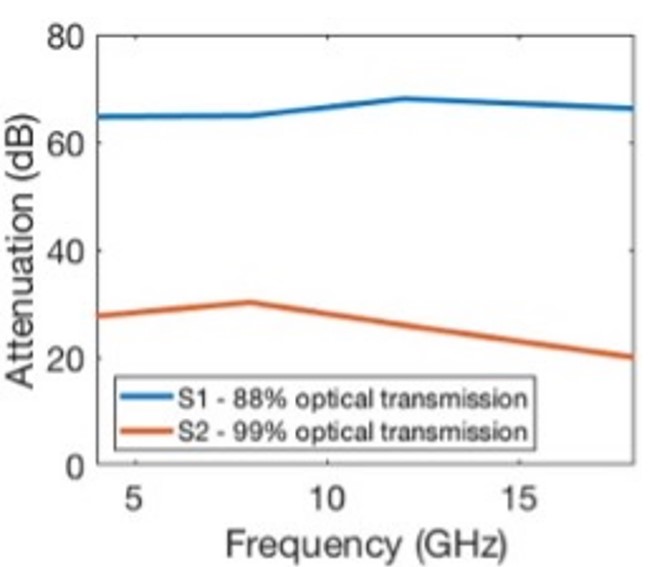
Figure 2 shows the SE measurements for two NANOWEB designs, S1 and S2. It is apparent that the high (60–70dB) EMI shielding capability of S1 is not achieved at the expense of optical transparency (approximately 90%). Source: Meta Materials Inc.
RML can effectively address the problem of discernible wires associated with the current MWM-based EMI shielding technology. Typically featuring a linewidth that does not exceed one micron, NANOWEB fabricated using RML is impossible to see with the naked eye, thereby offering a significant transparency improvement on industry-standard perforated metal screens or micron-scale MWMs.
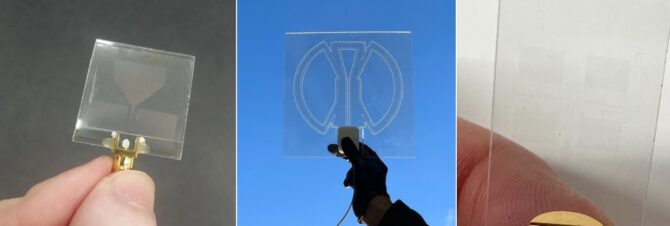
Figure 3 shows three working prototypes of transparent antennas developed using NANOWEB. At left is a monopole antenna, operating at 6–10GHz. In the middle is a large indoor digital television (TV) reception antenna, which operates at 400–800MHz. The rightmost antenna is a four-array element patch that operates at 5G mmWave bands between 26 and 28GHz and is compatible with modern 5G networks. Source: Meta Materials Inc.
Transparent antennas
Another notable application of NANOWEB is optically transparent antennas. Transparent antennas are useful for integrating antenna functionality into transparent surfaces, such as windshields and windows, while maintaining visibility.
High transparency in these antennas is attained without sacrificing the electromagnetic behavior. This key benefit, along with minimum installation space requirements, propels them to the forefront of antenna choices for many application scenarios. They include 5G antennas for smartphones, smartwatches, and vehicles; Bluetooth antennas for wearables and Internet-of-things (IoT) devices; and satellite antennas mounted on solar panels.
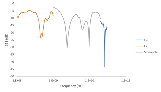
Figure 4: Measured frequency responses of NANOWEB transparent antenna prototypes. Source: Meta Materials Inc.
With both aesthetic and space advantages over traditional opaque and obtrusive options, NANOWEB transparent antennas, designed for the frequency range from 400MHz to 92GHz, are anticipated to play a significant role in next-generation telecommunications infrastructure.
RF redirection films
As the backbone of smart cities, ubiquitous and reliable connectivity relies on extensive, high-performance (5G/6G) wireless cellular networks capable of handling vast numbers of simultaneous connections with low latency and high data speeds.
Known for high directivity, short ranges, and susceptibility to obstruction, RF communication signals present unique challenges for realizing full network coverage in dense urban areas. The increasing adoption of windows made of energy-saving low-emissivity glass in modern buildings also impedes signal transmission as these windows cause considerable signal attenuation.
Countering this impediment, additional network infrastructure is deployed to improve network coverage, but this is a costly and space-demanding approach. Moreover, network towers are becoming increasingly objectionable to city residents, often devaluing their real estate.
NANOWEB-based RF redirection films present a passive and more sustainable alternative solution for eliminating wireless dead spots. Applicable virtually anywhere, these ultra-thin, transparent, and flexible films can selectively transmit and/or reflect signals in the sub-6-GHz and mmWave ranges.
For factories and hospitals where wireless IoT devices and tools are increasingly employed, another added advantage of passive redirection over-active signal relay is that the passive solution does not add any electronic signal lag. Traditionally, relaying a 5G signal through a building with many corridors and rooms may add seconds of nonuniform signal delay, an important consideration in circumstances where all IoT devices may need to work in unison.
Deicing/defogging
As a one- or two-dimensional nanowire-based film configured as a resistant heater element, NANOWEB can deliver uniform heat in a variety of novel high-performance applications. From eyeglasses to windshields, the ability to ensure constant visibility in inclement conditions like fog, ice, and snow is ever more critical.
Next-generation automobiles, especially those now employing advanced driver-assistance system (ADAS) levels 3, 4, and 5, will use 20 or more scanners and sensors, all requiring sensor signal visibility. With growing driver reliance and the ever-pressing demand for vehicle safety, sensor heaters must react fast and be transparent and uniform to ensure maximum signal-to-noise integrity in all inclement conditions.
Owing to its low resistance, NANOWEB can achieve the power density required for heating applications with low voltage. For example, as a heating element for windows, NANOWEB can reach up to 70°C in less than a minute with 12 volts or less applied.
Condensation occurs when water droplets form as warm air comes in contact with a cold surface. This phenomenon is particularly problematic for masks and eyewear as it drastically reduces visibility. Heating can effectively address this problem by eliminating the temperature gradient between the mask/eyewear lenses and the surrounding air. Compared to other film-based heating solutions (e.g., ITO), NANOWEB is more efficient at defogging due to a heat density as high as over 10,000W/m2, while maintaining high transparency.
In addition, use of automotive RADAR sensors is completely blocked by conventional ITO heaters, whereas NANOWEB linear one-dimensional nanowire arrays are polarized, allowing 100% RADAR transmission. These arrays are impossible to be patterned on ITO invisibly. For LIDAR, the high optical transmission afforded by NANOWEB results in significant signal-to-noise real-world detection, building a higher-resolution point cloud and realizing environmental detection so critical to ADAS level 4 and 5 autonomy.
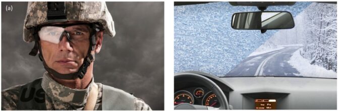
Figure 5: NANOWEB-based anti-fog eyeglasses and windshield deicing systems. Source: Meta Materials Inc.
Conclusion
Composed of a precise arrangement of submicron metal wires that are imperceptible to the human eye, META’s NANOWEB offers a flexible, cost-effective, and sustainable alternative to conventional transparent conductive materials. Exceptional, highly differentiated electrical and optical properties, combined with complete customizability with Rolling Mask Lithography (RML) and ready adaptability, make this ultra-thin, transparent, conductive film a breakthrough solution for wide-ranging applications like 5G, automotive, and consumer products alike.
————————-
Based in Dartmouth, Nova Scotia, Meta Materials Inc. designs, develops and manufactures sustainable, high-performance, functional materials for a wide range of applications.
https://metamaterial.com/products/nanoweb