The case for diamond semiconductors
By Adam Khan, founder & CEO, AKHAN Semiconductor
Electronics Semiconductors Supply Chain diamond diamond Miraj Miraj platform platform semiconductor semiconductorNewly developed technology aims to impact and transform all industries
As we continue to enhance the technology within our electronics to create devices that are smaller, more powerful and more energy-responsible, we’ve begun implementing Wide Bandgap (WBG) semiconductors. With their ability to operate at temperatures of over 300 degrees, handle 10 times higher voltages and operate with over 90 percent increased power efficiency, WBG semiconductors have the potential to save billions of dollars in energy and cut the cost of electronics.
Wider bandgap semiconductors operate at 300-degrees C, handle 10-times higher voltages and operate with more than 90% increased power efficiency.
While the implementation of WBG semiconductors is the first step towards better electronic devices, the next is determining which semiconductor material is the most effective. Thus far, silicon has been the predominant material of choice for semiconductors, despite its physical limitations for both computing and powering applications. Today’s applications require lithography feature sizes approaching the atomic limit for silicon in computing, and higher blocking voltages, switching frequencies, efficiency, and reliability in power.
It’s time to adopt a new standard for WBG semiconductor material, one without limitations and one that will augment the already impressive capabilities of WBG semiconductors.
What materials are top contenders?
The top three materials for WBG semiconductors are diamond, silicon carbide and gallium nitride.
Diamond is a leading contender with its ability to significantly outmatch other materials in a variety of properties, including applicability with new doping approaches and low temperature growth (CMOS compatible). However, it’s inhibited by the process necessary to make it fit for electronics. Being the least mature of WBG semiconductor materials, development work is needed on commercial semiconductor processes to enable widespread applicability and high-volume usage.
Silicon carbide (SiC) is the most mature/familiar of the WBG semiconductor materials. Despite higher processing temperatures (700C) and costly substrates (single crystal silicon), the long maturation cycle of the technology has made it the cheapest of the three WBG semiconductor materials. SiC has broad commercialization in power devices and electric and hybrid electric vehicles (EV/HEV) markets due its higher operating temperature even at higher voltages. However, high deposition temperatures and limited substrate applicability still leave SiC bounds away from the CMOS silicon platform.
Gallium nitride (GaN) is more mature than diamond and GaN devices have had widespread deployment in optoelectronics (LED and Laser Diodes), RF, and high-power electronics primarily due to the material’s direct bandgap and high-frequency performance. However, GaN remains the costliest of the WBG materials and lacks in thermal performance (one-fourth the thermal conductivity of SiC and one-twentieth of diamond) as well as power handling.
Why diamond?
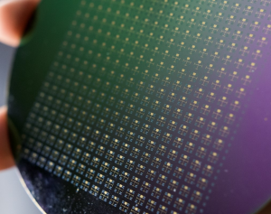
As the technology space entered this new frontier of WBG semiconductors, AKHAN Semiconductor was determined to identify the most suitable material for this application and refine it into a cost-efficient and effective solution in all major industries. Considering the untapped potential and widespread awareness of diamond’s inherent properties that allow for significant heat diffusion and transmission of large amounts of energy through small quantities, AKHAN developed its Miraj Diamond Platform.
Since diamond has long been inaccessible due to high costs and limited amounts of the material, through extensive research and scientific advancements, AKHAN created a state-of-the-art manufacturing process that enables us to produce these crystals at a low-cost using methane gas and plasma as source materials. These wafer scale processes utilize chemical vapor deposition (CVD) reactors to form diamond in nanocrystals below 400°C, enabling their integration with complementary metal oxide semiconductor (CMOS) devices, commercial display glass, and other materials previously precluded due to temperature sensitivity—creating the perfect diamond wafers needed for electronics.
Manufactured at the firm’s Gurnee, IL headquarters, the Miraj Diamond Platform is manufactured with tight control of quality and IP, serving mostly customers in the defense, consumer electronics, aerospace, automotive and telecommunications sectors.
Benefits of implementing diamond semiconductors include:
- Improved Heat Diffusion – Diamonds’ ability to conduct heat far surpasses that of materials currently used for electronics—unlike convection based cooling (e.g. fans) and heat sinks, diamond films can be directly integrated into a chip, which cools much more efficiently (direct phonon cooling) and much faster (with diamond thermal conductivity 22 times that of silicon and five times that of copper). Diamonds can also withstand and operate at temperatures over 600 degrees Celsius (versus 150 degrees Celsius for Silicon), meaning electronics can run hotter without expensive and bulky cooling requirements.
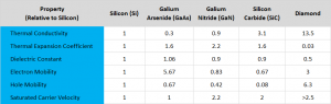
- Increased Power Flow – With diamonds ability to handle higher voltages than silicon without breaking down, new devices will be available for high power application such as Metal Oxide Semiconductor Field Effect Transistors (MOSFETS) and Schottky Diodes (where building higher-voltage-rating MOSFETs and Schottky diodes is limited due to the large silicon die increase as the breakdown voltage requirement increases, resulting in reduced manufacturing yields and increased costs). Today’s silicon systems can only utilize insulated gate bipolar transistors (IGBTs) and pin diodes both with higher loss than their mentioned counterparts. Not only can diamonds handle more power, but they also operate at over 90% increased power efficiency by reducing the ambient power loss compared to current technology.
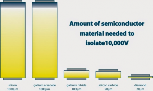
- Less Space Required – One of diamonds’ rarest properties is its uncommon ability to isolate massive voltages with just a small fraction of the material. Consider this, 50 times less diamond is needed than traditional silicon material when isolating 10,000V. With less material needed to transmit higher voltages, the lowest on-state resistance, the highest saturated drift velocity, and the highest breakdown voltage of all semiconductor materials, technologies that use diamond will be more than 1,000 times thinner than those that use silicon.
What are the applications of diamond semiconductors?
Diamond technology anticipates impacting and transforming all industries, with some of the most notable applications including:
- Faster supercomputers
- Advanced radar and telecommunications
- Hyper-efficient hybrid and electric vehicles
- Electronics in extreme environments
- Next-generation aerospace and avionics
- Faster, lighter, and more capable aircraft and propulsion
- Offensive and defensive capabilities in directed energy/high-energy laser systems
- Lighter and more durable consumer electronics
In the end, diamond technology enables users to develop faster, smaller and more energy efficient electronics at a lower cost.