Taking the temperature of the white-hot micro LED market
By Mark Ritzheimer, senior product manager, thermal products, Advanced Energy
Electronics Optoelectronics Supply Chain LED LED MicroLEDs MicroLEDsMicro LEDs have better performance over LCD displays, including significant higher resolution and contrast, better color saturation, lower latency and lower energy requirements.
What do laptops, mobile devices, flat panel display TVs, digital signage, automotive infotainment systems and augmented/virtual reality (AR/VR) headsets all have in common? Displays are the obvious answer, but there’s an additional nuance that electronic engineering and design firms can’t afford to overlook in this rapidly-changing technology landscape: the growing emergence and important of micro LEDs. In this Q&A, Mark Ritzheimer, Advanced Energy senior product marketing manager for photonic products, explains what the technology is and why it could enable one the fastest-growing markets through at least 2025.
The early phases of the MOCVD production process are critical and serve as the foundation of the Micro LED being produced.
What is micro LED technology?
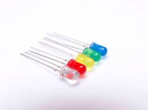
Micro LED is an emerging technology for flat panel displays for a variety of products, such as smartphones, laptops, automotive infotainment systems and TVs. The name comes from their microscopic size: from 50 µm to 2 µm, depending on packaging. Micro LEDs have better performance over LCD displays, including significant higher resolution and contrast, better color saturation, lower latency and lower energy requirements. Compared to traditional LEDs, there are an emissive diode, meaning that they also have the added benefit of generating their own light output built into the diode itself. Micro LEDs have the potential to deliver the higher quality and immersive experience of OLED displays, but at a lower cost.
What are its major benefits?
Compared to traditional, larger LEDs, micro LEDs provide better contrast and higher energy efficiency. These and other advantages make micro LEDs a great fit for devices that are frequently used around high ambient light, such as automotive infotainment system displays or digital signage. Their higher energy efficiency also makes them ideal for battery-powered devices, such as laptops and smartphones.
Another example is consumer TVs. Many TV manufacturers see micro LEDs as a way to deliver OLED picture quality and a more immersive experience, but they’re expected to deliver this technology at a lower price point because they’re manufactured used existing LED manufacturing technology and infrastructure. Samsung is among the household names currently developing micro LED TVs and other products for consumers and businesses.
Although it’s a relatively new technology, the micro LED display market already was worth $272 million in 2018, according to Zion Market Research. By 2025, it will hit $21.1 billion. That’s a compound annual growth rate of over 86 percent.
How are micro LEDs manufactured?
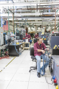
Micro LEDs are manufacturing, or you might even say “grown,” in large-scale reactors that employ metalorganic chemical vapor deposition processes, or commonly known as “MOCVD.” These reactors produce LEDs in large batches using multiple wafers and series of deposition techniques that are controlled by temperature and gas flow of reactants into the chambers. Many of the existing reactors that are already in use around the world make to product traditional LEDs can be quickly and cost-effectively converted to produce micro LEDs. But when they’re making that transition, manufacturers must upgrade also upgrade some of the in-situ measurement equipment used to control critical parts of this production process. One of the most important is around temperature measurement and control, and the use of optical temperature pyrometers. These pyrometers precisely measure temperature and are necessary for maximizing yields and profits.
To understand why, let’s look at how MOCVD reactors work and how their temperatures are measured. Reactor pyrometers traditionally used 940 nm wavelengths to measure the temperature susceptor, or the carrier, that holds the wafers that are being processed. The catch is that at 940 nm, the pyrometer can’t “see” the sapphire wafers for the LEDs are actually grown, or some of the thin films that are being deposited, so it can’t precisely measure their temperatures during steps of the production process.
Instead, the pyrometers do the next best thing: measure the carriers’ temperatures and extrapolate from that to estimate the wafers’ temperatures. This measurement technique has been state-of-the-art for many years, and has been made to work for traditional LED growth, but does not provide the more precise temperature measurement and control needed for the production of the more sophisticated micro LED structure.
In an effort to upgrade these capabilities, LED manufacturers began exploring the use of a “shorter” wavelength with their optical temperature pyrometers that provided new insight into their process. By selection a different measurement wavelength, around 400-430 nm, this shorter wavelength enables pyrometers to see the wafers throughout the entire production process, from start to finish.
One of the greatest challenges for optical temperature pyrometers measuring at these shorter wavelengths is the limited thermal radiation being emitted, which makes the measurement more difficult, especially at some of the critical temperatures necessary for the growth of micro LEDs. Pyrometers in this space not only have to be able to measure correctly at these shorter wavelengths, with limited energy, but simultaneously being able to delivery razor-sharp performance. This is no easy task and has been a barrier for some LED growth processes. But AE is able to delivery an optical temperature measurement pyrometer measuring at 425 nm, that only is able to measure directly the exact and critical steps needed for microLEDs, but also with the resolution, repeatability and accuracy required for the most demanding microLED processes. This leads to greater process control, uniformity of product and overall yield of each batch process.
Why is temperature control so critical with micro LED manufacturing?
The early phases of the MOCVD production process are critical, and serve as the foundation of the Micro LED being produced, and have direct correlation to the results emittance of the microLED. Direct measurement of the sapphire and early layer growth significantly increases micro LED uniformity and repeatability, and maximizes yields, which in turn maximizes profits.
For example, even a small error in processing temperature – even less than 5C – can result in a colour shift in the LED. A 400-430 nm pyrometer can monitor temperatures from start to finish, which enables the manufacturer to meet these tighter requirements throughout their entire production process. That means less binning and less waste because manufacturers have a better chance of getting the wavelengths they want.
What is the business model and how does the tech impact the bottom line?
As current LED products make the transition from traditional LEDs to micro LEDs, many of them will do this using existing MOCVD reactors and upgrade the instrumentation with the equipment to make this transition possible. There is also a learning curve in this process, as chambers are converted and production recipes not have to be rewritten to accommodate for micro LED growth, but manufacturers will have to perfect the recipes and incorporate years of learning into this transition. This is no easy step, and the LED producers who can make this transition more easily and efficient may lead the pack, and gain a competitive advantage and faster time to market. A way of helping make this successful is by upgrading these chambers with the hardware necessary, like AE’s UV400 425 nm optical temperature pyrometers, to enable more precise control and speed this learning and development cycle.