Could printed copper become the new industry standard?
EP&T Magazine
Electronics Production / Materials C2MI copper ETS materials pcb pcbs printed productionMultiple advantages, convincing results could prove to be the case in microelectronics manufacturing
The recent results obtained by a team of Canadian scientists made up of members from academia and industry and based at C2MI – Canada’s largest microelectronics R&D centre – may lead to achieving greener, more sustainable products, by scaling up and enabling technological boundaries to be pushed back and broadened.
C2MI recently joined the Semiconductor Climate Consortium, with the clear intention of offering new avenues in microelectronic products manufacturing. The consortium is focused on the challenges of climate change and works to speed industry value chain efforts to reduce greenhouse gas emissions in member company operations and in other sectors of our value chain.
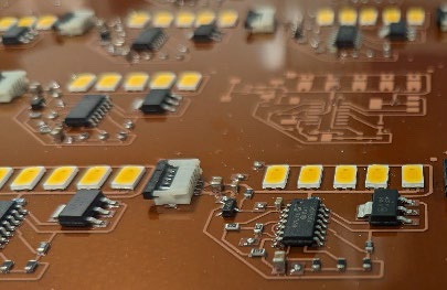
C2MI copper-based printed circuits.
In the flexible electronics world, two options are available, including flexible circuits manufactured with traditional pcb technology. These copper circuits provide good reliability, but requires harsh chemicals to manufacture and these subtractive processes waste a lot of copper. Printed circuits technology is also available, but mainly with printed silver circuits which are costly and have the disadvantage of suffering from electromigration during the product’s life affecting the reliability of the device. While new printing technology is offering more versatility, no one is ready to give up on reliability nor experience higher production costs. That is why the aim of this project has been to create a solution that would have the advantage of both worlds. The printed copper solution presented in this paper have reliability similar to traditional pcb technology with the advantage of using additive technology to prevent copper waste and the use of harsh chemistry.
C2MI is equipped with industry equipment which enables pilot production on production ready equipment to ensure a smooth transfer of developed technologies onto larger volume product lines once the developed new products are ready for volume commercialization and manufacturing.
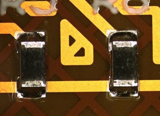
Copper foil based flexible printed circuit boards (F-PCB). Source: C2MI
The printed electronic tests were conducted in a manufacturing process mode targeting optimal and reliable results such as those that are conventionally widely obtained in the industry. The new copper-based printed electronics flexible circuits are indeed meeting the JEDEC JES022-A110 standard while reducing considerably copper loss, chemical consumption as well as significantly reducing the overall costs compared to traditionally used subtractive processes. The printed technology selected is as close as possible to readily available technology: copper-based circuits are widely used with rigid boards. The assembly process used with this new copper printed flexible electronics utilizes the same equipment present in a standard card attach line as to streamline the transfer of that technology to existing assembly plants.
Therefore, copper printed circuits were selected as the best option for the following advantages:
- Reducing chemical consumption compared to current pcb technology: Printed circuit board manufacturing is currently made with subtractive processes. These processes require harsh chemicals such as copper etching solutions. Direct printing of circuits doesn’t require those harsh chemistry and consume less copper per unit manufactured compared to the subtractive processes currently used within the industry.
- Meeting the standards: copper is a documented reliable material and show no signs of electromigration during reliability testing. Wetting is one of the criteria of IPC standards for quality control. With our printed circuit technology, we obtain wetting that would be acceptable under IPC-A-610. Testing was also done after assembly and the circuits were having similar energy consumption and LED output compared to an available flexible circuit manufactured with traditional pcb technology.
- Reducing the overall costs of printed products: Reducing the cost of inks by more than 50% in comparison to silver inks. Using copper printed traces instead of silver enables the use of solder paste as component attach material. Solder pastes are widely used in the card attach industry and are between 10 and 100 times cheaper than component attach materials commonly used to attach components on silver traces.
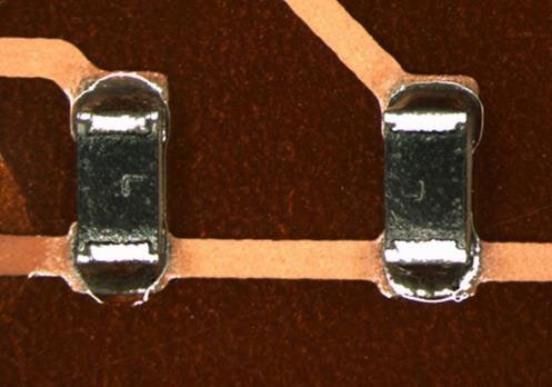
Copper circuits printed on flexible polyimide. Source: C2MI
This new technology has the advantage of both solutions present on the market namely the advantage of a printing technology that doesn’t rely on harsh chemicals, cut costs, and minimize waste through an additive process instead of a subtractive one. All of this is achieved while maintaining the same reliability obtained with currently used pcb technology. This new technology is a great example of what C2MI has at its core value, providing a solution to customers that are low cost, reliable and with less waste.
————————————-
The study was performed by C2MI and ETS, involving a close collaboration between Sylvain Cloutier Professor and Chair of the Electrical Engineering Department at École de technologie supérieure (ETS) Canada Research Chair in Printable Optoelectronics Materials & Devices and Christophe Sansregret, Process development engineer in printed electronics and microelectronics assembly at C2MI along with a team composed of ETS Students ( Arjun Wadhwa, Alain Picard, Luis-Felipe Gerlein, François-Xavier Fortier, Debika Banerjee, Jaime Benavides and Alexandre Perroton) as well as C2MI team members (Julien Néron and Sylvain Yergeau), features conclusive results.