5N Plus achieves supply deal with Samsung
EP&T Magazine
Electronics Semiconductors Supply Chain materials Samsung semiconductors supplyArrangement for engineered substrates for next gen medical imaging systems
5N Plus Inc., a Montreal-based producer of specialty semiconductors and performance materials, announced a long-term agreement with Samsung Electronics Co. to supply engineered substrates based on II-VI semiconductor materials for the detector core of the next generation of medical imaging devices. The detector is based on Photon Counting Detector (PCD) technology, and will be incorporated into computed tomography (CT) by Samsung’s subsidiary NeuroLogica Corp., located in Danvers, Massachusetts.
Market driver for PCD technology
The global market for medical imaging based on CT is estimated to over five billion dollars in revenue. The detector element comprises 5 to 10% of the cost associated with the device. Over 95% of the CT imaging devices produced today are non-PCD-based. The increased demand for enhanced diagnostics, radiation reduction and cost efficacy have made this market ripe for innovation. PCD technology is at the forefront of addressing the latent demands associated with this market. In recent years, the advancements in product and process technologies have delivered PCD-based imaging systems with superior image quality and reduced radiation levels not achievable with the current mainstream technology.
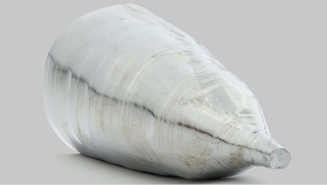
5N Plus manufactures class leading high purity, Indium Antimonide wafers that provide improved resistivity, uniformity and lowers defects through a unique crystal growth method.
Collaboration delivers breakthrough tech
Over the last several years, 5N Plus has been developing engineered substrates for high-performance detectors essential for applications in medical and security markets. These efforts have recently yielded a family of semiconductor substrates facilitating unrivalled performance in both PCD-based CT imaging and various applications within the security market. Through its close collaboration with Samsung and NeuroLogica, 5N Plus has developed an engineered substrate product optimized to uniquely fulfill requirements for PCD-based CT medical imaging devices. The success of this program has prompted both parties to engage in a long-term supply relationship.
“We are very pleased by the outcome of this project and believe 5N Plus is uniquely positioned to become the leading global supplier of engineered substrates for PCD-based medical imaging applications,” said Arjang Roshan, President and Chief Executive Officer of 5N Plus. “We would like to thank Samsung and NeuroLogica for cultivating a collaborative ecosystem which not only fostered innovation but enabled its expedient implementation.”
Expansion of specialty semiconductor value-chain
5N Plus continues to expand its value-chain for specialty semiconductor materials. With over 20 years of experience in the development and manufacturing of ultra-high purity II-VI semiconductor compounds, the Company is the leading global supplier of these products. Over the past several years, 5N Plus has expanded its value-chain through its site in St. George, Utah, utilizing these compounds to develop engineered substrates. These efforts have resulted in an array of engineered substrates facilitating unsurpassed performance in customer applications ranging from PCD-based solutions in medical imaging to engineered substrates for infrared imaging and other applications within the security industry.
Recently, the Company announced that it is investing $8.5 million in its Montreal campus to expand the development and manufacturing of critical and strategic materials, including those containing tellurium, for advanced II-VI semiconductor compounds and engineered powders. The investment is supported and has received funding from governmental agencies for about a third of the total investment.