In-mold electronics gets human touch
By Ron Haag, VP of technology & Julie Ferrigno, R&D engineer, E2IP Technologies
Electronics Optoelectronics Printable Electronics Wearable Technology Editor Pick Electronics Flexible HMI in-mold printed wearableMontreal smart surface solution specialists work with NRC on 5G
As printed electronics become integrated into industrial and commercial products and solutions, the term ‘printed electronics’ is now mainstream. While leveraging printed electronics, e₂ip technologies, has been working in partnership with the National Research Council of Canada (NRC) to advance the material science and manufacturing of In-Mold Electronics and with the Communication Research Centre of Canada (CRC) to develop it’s 5G smart surface technologies. This article offers an overview of these technologies.
What is in-mold electronics?
Source: e₂ip technologies
In Mold Electronics is becoming a common buzzword in the human machine interface (HMI) industry. Understanding the intricacies between the design and the process of producing a finished IME product is not that common, therefore a simplified explanation will help to understand the benefits of the technology.
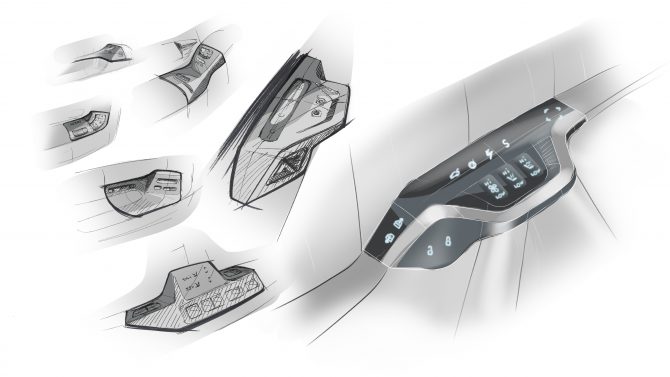
Industrial design
The IME design begins with the creation of a 3D surface via industrial design experts that have vision and intuition as to how a user interacts with a device. From touch, to lighting, to material selection and integration into its surrounding environment, all these attributes go into creating the desired look and feel. This makes surfaces smarter to simplify our everyday lives.
Engineering
Once the part is designed in a CAD model stage, the design is recreated in a 2D format. This is the point where the engineer(s) will step in and utilize electronic skills, printed electronic expertise, connector methods, and lighting techniques combined with printing techniques to create a sophisticated version of a circuit board on a thin plastic film substrate utilizing specialized formable conductive and non-conductive inks.
Manufacturing
When the circuit and graphic designs are completed the actual manufacturing processing steps begin. The first process step is the printing phase which requires understanding the ink chemistries and print layer stack-ups. In some cases, the overall print stack-up is completed on a single film and in others two films are used.
The second process step includes the pick-and-place of components required to add LED’s, passive components and in some cases microprocessor capabilities. It should be noted that depending on the types of ink used, the pick-and-place step could move to a later point in the process.
The third process step converts the flat printed sheet to its intended 3D user interface shape. All inks along with the components on the film end up being positioned exactly where intended in the final shape of the part. Typical thermoforming methods include high pressure forming and in some cases vacuum forming. The films are trimmed, sometimes before molding and sometimes after molding, and the circuits are function checked. Molding is the final process consisting of placing the formed films in a mold, where the resin is injected between the films to encapsulate all the components. This also provides the part with its rigid structure and a means for attachment via screw bosses or clips.
Finished product
IME represents the future of HMI in several industries including but not limited to aerospace, automotive, medical, white goods and industrial. IME offers industrial designers the freedom to create a truly innovative user interface with a smooth curved surface that integrates seamlessly into its surroundings. Finished parts are thin, lightweight, durable, cost efficient and highly reliable. Additionally, they are easy to assemble with a streamlined manufacturing process, lower cost of assembly, and a lower carbon footprint.
e₂ip technologies extended IME offering is called ‘smart molded parts’ and can include capacitive touch switches, various illumination techniques, proximity sensors, printed heaters, antennas, and shielding techniques.
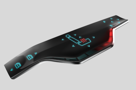
Molding is the final process, where resin is injected between the films to encapsulate all of the components. Source: e₂ip technologies. Source: e₂ip technologies
5G smart surface
This technology is unique among e₂ip’s printed electronics product offering in that it does not have a human machine interface (HMI) application.
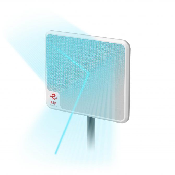
To look at, this technology could not be simpler. An e₂ip 5G smart surface is a fine line pattern printed on a thin, flexible substrate. The design of the pattern predicates the functionality.
Signal redirection applications
Source: e₂ip technologies
To start we must recognize the basic properties of millimeter-wave propagation. Due to the short nature of the wavelengths, these signals cannot cover large areas or pass through, buildings, walls, trees or solid structures. Due to this, millimeter-wave 5G networks will always have ‘dead zones’, particularly in dense city configurations. In order to extend coverage to these ‘dead zones’ providers deploy small cell antennas. These antennas require power to operate and considerable resources for installation. 5G smart surfaces are a passive, require no power, and are low cost alternative to replace a proportion of the overall number of small cell antennas required in a 5G network, depending on the network design and requirements.
Because this technology is passive, installation is relatively simple. An e₂ip 5G Smart Surface is applied to a surface and positioned in line of sight of a 5G signal to redirect the signal in a pre-set direction. The surface could be a wall, window, billboard, a painting or a custom panel. The dimensions vary based on design and network requirements.
Different patterns provide different functionality. For signal redirection, the 5G smart surface (reflector) can act as a mirror for a selected frequency and redirect the signal at a specific angle. While the 5G smart surface (diffuser) re-directs the signal in multiple directions. The diffuser technology is used to cover dead zones inside buildings or to enhance the coverage of the 5G Network outdoors in dense cities.

From ideation to fabrication, Montreal-based e₂ip Technologies delivers HMI and smart surface solutions to global market leaders. Source: e₂ip technologies
Signal blocking applications
e₂ip’s 5G Smart Surfaces can block certain frequencies and ignore all others. This technology can be leveraged to protect the data transmission at a certain frequency from one space to another or act as a shield, preventing certain millimeter-waves from propagating.
Both mechanically and functionally the surfaces can be customized to meet each customer’s specific needs. This technology has been designed and is qualified to perform in harsh outdoor conditions.
———————–
From ideation to fabrication, e₂ip technologies delivers innovative human-machine interface (HMI) and smart surface solutions to global market leaders. Montreal-based firm are specialists in printed electronics, material science, advanced manufacturing processes and embedded system development.