How to prepare for wide-bandgap semiconductors
By Jonathan Tucker, power market segment manager, Tektronix
Electronics Semiconductors Test & Measurement Engineering Editor Pick GaN MOSFETs power semiconductors SiC Tektronix test WBG wide-bandgapEmerging technologies deliver on power efficiency, new challenges for engineers
Higher power performance inside a smaller form factor is now required in a number of sectors, such as data centre power supplies, automotive powertrain, battery management systems, grid energy storage, rail, emerging aircraft, and more.
The power-density advantages of smaller designs are evident in mobile deployments, but compact power electronics also have the potential to reduce overall system cost as smaller, more light-weight components can correspond to lower capital and operating expenses. The added need for greater energy efficiency is being spurred by both an operational desire to lower costs and by regulatory demands around the world.
Figure 1: Power losses shown at the point of generation, transmission, and consumption. Source: Tektronix
Size vs. efficiency
The design challenge is that the goal of reducing physical size often competes with the goal of increasing energy efficiency. For example, increasing the switching frequency of converter circuits allows the size of components such as inductors, transformers, and capacitors to be reduced. That helps enable more compact devices at lower production cost. But, higher switching frequencies also generate additional heat and the risk of electromagnetic interference.
The effort to boost device density and performance while reducing power consumption has led to research into unique two-dimensional solids with high carrier mobility and higher conductivity. While the desire for greener power generation solutions is spurring investigation into higher temperature superconductors and the power semiconductors essential to power conversion.
GaN & SiC
Traditional silicon technology is based on narrow bandgap material, which leads to undesirable conductive leakages that become more pronounced with increases in temperature, voltage, or frequency. New wide-bandgap (WBG) semiconductors such as gallium nitride (GaN) and silicon carbide (SiC) have much higher power density, smaller size, better high temperature performance, higher frequency response, lower leakage, and lower ON resistance than silicon, all of which add up to greater operating efficiency.
GaN has driven a reduction in size while increasing power density, helping to improve everything from the battery charge time to power supplies and amplifiers. SiC metal-oxide-semiconductor field-effect transistors (MOSFETs) are capable of operating at higher voltages and higher temperatures suitable for power transmission, large-scale HVAC equipment, and industrial systems.
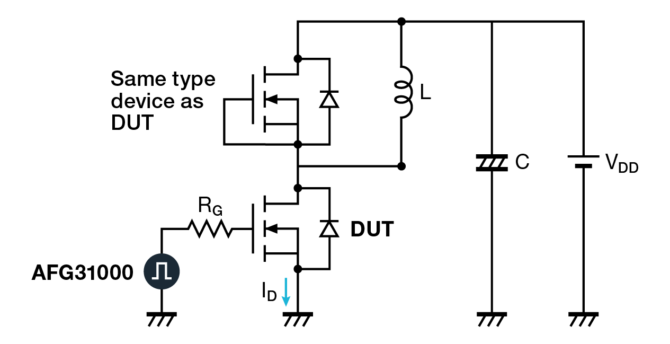
Figure 2: Double Pulse Test Circuit. Source: Tektronix
New capabilities & challenges
To fully embrace these new opportunities, testing and validation engineers need to reduce and simplify their measures while also increasing accuracy.
There are three specific processes which can be improved when working with WBG devices:
DPT
The standard test method for measuring switching parameters and evaluating the dynamic behavior of SiC and GaN MOSFETs is the double pulse test (DPT). DPT is performed using two WBG devices. One is the device “under” test (DUT) and the second “high” device is typically the same type. The inductive load is on the “high” device and used to replicate circuit conditions in a converter design. For the test, a power supply or source measure unit supplies the voltage, an arbitrary function generator (AFG) outputs pulses that trigger the gate of the MOSFET to start conduction of the current, and an oscilloscope measures the resulting waveforms.
Historically, it has been a time-consuming process to set up because function generators do not usually have a built-in way to configure and set up the test. Thankfully, newer AFGs include built-in software applications that enable DPT from a touchscreen interface.
I-V characterization
Similarly, current versus voltage (I-V) characterization to show the relationship between the current flowing through an electronic device or circuit and the applied voltage across its terminals has been a fundamental, but cumbersome method of understanding the potential of WBG semiconductors.
Today, many of the key measurements for characterizing WBG devices such as current vs. voltage testing, breakdown voltage testing, and leakage current testing are available through graphical Source Measure Units (SMU) and semiconductor parameter analyzers with user interfaces and application software that makes the process much easier.
Figure 3: I-V Curve Tracer Configurations. Source: Tektronix
Floating differential measurements
Finally, a typical switch-mode power supply might have an efficiency of about 87%, meaning that 13% of the input power is dissipated within the power supply, a significant portion is in the switching devices, usually MOSFETs or IGBTs. To reduce this loss, engineers may conduct floating differential measurements, such as high-side Vgs. These measurements, however, are difficult to make due to high frequency (fast turn on and turn off), and the presence of high common mode voltages (such as Vds) because oscilloscope probes do not have sufficient common mode rejection at high bandwidth.
This poor common mode rejection leads to the measurement being dominated by the common mode error instead of the actual differential signal. Isolated probes that do not de-rate with frequency at the operating requirements of GaN and SiC devices allow for more accurate differential measurements to precisely calculate and prove conduction losses, dead time losses, and switching losses.
Preparing for future devices
The new challenges engineers face with WBG devices certainly do not outweigh the benefits. As additional research is being conducted on other materials, such as aluminum nitride (AlN), gallium oxide (Ga2O3), and diamond, engineers will likely find more opportunities to improve testing.
By better understanding why WBG devices are growing at scale, where they will be deployed, and how they are measured and validated, engineers can be prepared to take advantage of smaller designs and greater efficiency that multiple segments now require.
——————————
Tektronix has more than 70 years of experience designing industry leading test and measurement equipment for the electronics industry.

Jonathan Tucker, power market segment manager, Tektronix