U of Sherbrooke launches research centre for nano semis, flexible opto
EP&T Magazine
Electronics Optoelectronics Semiconductors Engineering Environmental Supply Chain chair Flexible lab nano optoelectronics research semiconductors Umicore university-of-sherbrookeUmicore partners on research chair for semiconductor nanomembranes and flexible optoelectronics
The University of Sherbrooke recently unveiled its Umicore Research Chair for semiconductor nanomembranes and flexible optoelectronics. The initiative is headed by two researchers from the Quebec university’s Faculty of Engineering, members of the Interdisciplinary Institute of Technological Innovation (3IT) and LN2, Professors Abderraouf Boucherif and Richard Arès.
Partnered with global circular materials technology group Umicore and backed with five years of $1.5-million of seed funding, the associated research is aiming to transform optoelectronic and quantum applications by creating flexible, low-cost devices, without loss of performance. The challenge: current devices are manufactured on substrates that are incompatible with the new needs identified, in particular because of the thickness of substrates, along with its rigidity and mechanical fragility.
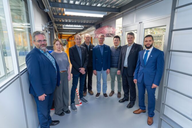
From left are Vincent Aimez; Laurie Mouchel; Jean Proulx; Paul Charette of University of Sherbrooke; with Kristof Dessein and Jinyoun Cho of Umicore; as well as Richard Arès and Abderraouf Boucherif from Uof Sherbrooke. Photo source: Michel Caron, University of Sherbrooke
The solutions to these challenges could, eventually emerge directly from the Sherbrooke laboratories, as the Chair will be able to support more than $8 million in related research. The chair will seek to enhance its own PEELER technology, enabling a “revolution” in several quantum and optoelectronic applications, according to Prof. Boucherif, co-holder of the chair.
“The PEELER method will allow us to reuse the substrate of a rare material several dozen times instead of a single use. For example, if we deposit a thin layer on a germanium (Ge) substrate, it can literally confer its special characteristics, its crystalline properties, to the thin layer,” said Boucherif. “This nanomembrane, now with new properties, can then be detached and then glued to another less rare and more accessible substrate, such as silicon. The advantages of these new production methods would be numerous: more economical, more sustainable, with a significantly smaller ecological footprint.”
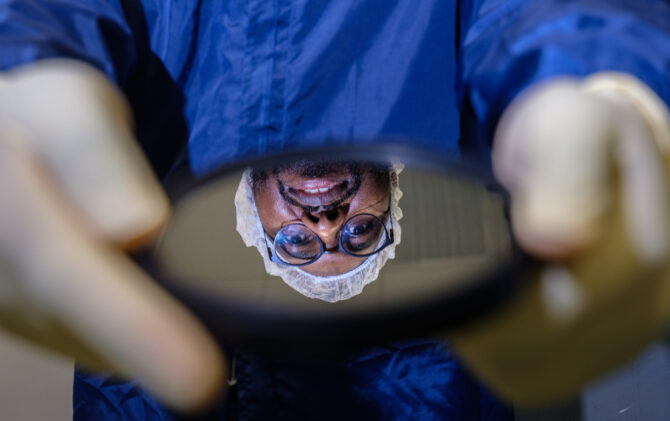
Photo source: Michel Caron, University of Sherbrooke
New mechanically flexible devices could soon emerge thanks to optimized development of flexible electronics. Rollable screens, medical devices that mold to biological shapes, photovoltaic cells that adapt to airplane wings or satellites, watches that adjust to the shape of the wrist: the numerous applications of flexible semiconductors could extend to technological deployments not previously considered.
Professor Richard Arès, co-holder of the chair, believes that the nano-microelectronics industry has always been seen as very environmentally unfriendly and that there is currently a lot of pressure on the cost of components.
“We will try to change that, he plans. Ge substrates are currently used in space solar cells thanks to its sought-after characteristics. So, we take this material 100 times rarer than gold, use it in a single application, send it into space and never see it again. This is where we can intervene. Reusing a super precious material is truly optimal for future generations and is a rare phenomenon in the industry. A Ge substrate 500 micrometers thick could allow the creation of 500 Ge nanomembranes ready to be deposited on other substrates. An entire global market has just opened up,” enthused Arès.
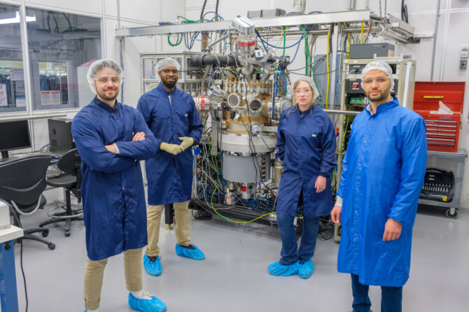
Posing with the Epitaxy equipment are Valentin Daniel, Thierno Mamoudou Diallo, Laurie Mouchel and Prof. Abderraouf Boucherif. Photo source: Michel Caron, University of Sherbrooke