How EMI shielding is enabling compact electronics
By Dr Yu-Han Chang and Yulin Wang, IDtechEx, Oxford UK
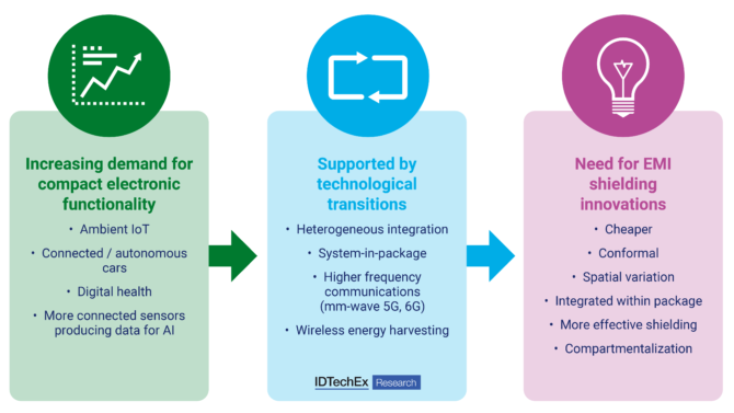
Circuit Protection Electronics Production / Materials circuit protection EMI shieldingIt is no secret that electronic devices are becoming increasingly compact, with greater functionality contained in smaller volumes. As such, increasing efforts are being made to mount integrated circuits (ICs) and other components such as antennas closer together, sometimes within the same semiconductor package. This proximity means that conventional board-level shielding of electromagnetic interference (EMI) with metal enclosures is being replaced with package-level shielding, with metallic coatings applied directly to semiconductor packages.
Increasing demand for compact electronic functionality. Source: IDTechEx
Conformal package-level shielding is especially important for consumer devices where both ness and wireless communications are needed. These include smartphones, smartwatches, and AR/VR headsets. By analyzing a range of teardowns, the report identifies the types of IC packages with conformal shielding and forecasts the market for conformal EMI shielding across multiple applications.
Emerging deposition methods
At present, sputtering is the dominant method of creating conformal EMI shields. Deposition occurs in a vacuum chamber, with ions fired at a metallic ‘sputtering target’ to produce nanoscale metal particles that coat the package surface. While the capital equipment is expensive, the metallic sputtering targets are cost-effective, with many providers having existing systems installed.
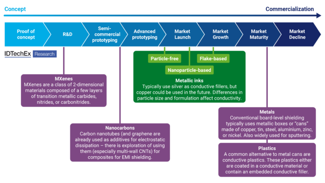
Concept to commercialization for EMI shielding. Source: IDTechEx
Emerging methods such as spraying and printing are gaining traction and offer much lower equipment costs since no vacuum chamber is required, along with additional benefits such as reduced variation in package top and side coating thickness and fewer process steps. However, conductive inks are typically more expensive than equivalent sputtering targets per gram of deposited material due to the additional ink formulation steps. The report evaluates the merits of different deposition techniques and discusses the key players.
An additional benefit of techniques such as inkjet printing is digital selective deposition, which enables reduced material consumption and hence mitigates the higher material costs of conductive inks. As the trend towards ‘system-in-package’ architectures gains further traction, greater use of compartmentalization will increase demand for selective deposition, such as the top of a specific compartment. In the longer-term, approaches such as fully additive 3D electronics will enable EMI shielding to be integrated throughout a complex bespoke package containing multiple compartmentalized components.
Material developments
While materials for board-level shielding enclosures, and indeed sputtering, are straightforward metals and metal alloys (typically copper, steel, aluminum, zinc, or nickel), there is considerable innovation within solution processable conductors for package-level shielding. Silver-based conductive inks dominate, with available products spanning a wide range of particle sizes and rheology. The report outlines the properties of competing conductive inks marketed at EMI shielding and the status of material innovations.
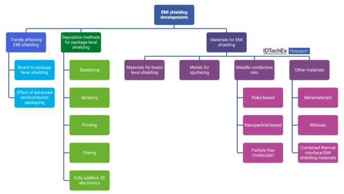
EMI shielding developments. Source: IDTechEx
Especially notable is the increasing adoption of particle-free (also known as molecular) inks, which are metalized in situ and hence produce smooth coatings and eliminate the risk of nozzle clogging. Metamaterials, in which periodic structures are introduced during manufacturing, can also be used to introduce frequency-dependent EMI shielding if desired. Another material alternative for solutions processable EMI shielding is MXenes. This term refers to a class of materials made up of metal carbides or metal nitrides that have excellent conductivity and are lightweight.
————————-
A recent IDTechEx report explores the current status and technology trends within this essential aspect of many electronic circuits. Based on IDTechEx’s expertise in evaluating developments within advanced semiconductor packaging and conductive inks, the report provides a comprehensive overview of the status, innovations, players, and opportunities within EMI shielding, focusing on developments at the package level.