Using chip antennas in pcb design
By Geoff Schulteis, senior antenna applications engineer and Robert Dumont, America’s sales manager, Antenova Ltd.
Electronics Wireless antennas antennas chip chip pcb pcbNB-IoT products are being implemented into many applications, including wearable electronics
Antennas are effectively transducers, turning electrical energy into radio waves and back again. This process involves physics, so the laws of physics are at play. While digital and analog components may be placed anywhere you like, with an antenna, its position and operation will impact its performance greatly. For this very reason, it is recommended to think about the antenna first, i.e. selecting an antenna at the early stages of a new product design, so that the antenna design constraints can be considered, and then think about creating a layout that will allow the antenna to perform at its best
Antenna position on pc
Unlike a digital component, an antenna will not always perform exactly as the specifications quoted on the data sheet. There are several factors that can affect its overall performance, such as:
- Length of ground plane
- Other components in proximity
- Outer casing and its material
- Position within the device
- Layout of the pcb (power/noise issues)
With any antenna, it is important to understand how its position will affect its performance. Particularly for an embedded antenna, the device needs to be positioned clearly away from the rest of the circuit – otherwise noise and other components can detune and interfere the component’s performance.
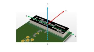
Figure 1 shows how the antenna radiates in six spatial directions.
Some antennas perform best when positioned on the corner of the pcb. However, there are other antennas that operate best along the long-side edge. The data sheet of each antenna will detail the optimum placement of the antenna, as will the design of the evaluation board.
The greatest design challenge is probably to provide sufficient ground plane length for sub-Gigahertz frequencies.
How the antenna radiates
A chip antenna radiates in six spatial directions and ideally requires clearance in three to five of these, as shown below. Where this cannot be achieved it is important to keep as many directions clear as possible, and at least a minimum of three. Where there are fewer directions clear, there will be a degradation of performance.
This is why some antennas perform best on the corner of a circuit board, as this effectively means there are five directions where the antenna can operate as if it were in free space.
Ground plane
Embedded antennas use ground planes on the host pcb in order to radiate efficiently. The ground plane constitutes half of the antenna, so respecting the recommendations provided in the manufacturer’s data sheets is essential, if you are to achieve good levels of radiated performance. In applications that require network certification, following the guidelines in the manufacturers data sheet for the selected antenna is critical.
There are two common configurations for the ground plane. In some cases, the ground plane extends under the antenna and in others there needs to be ground cleared away under the antenna itself.
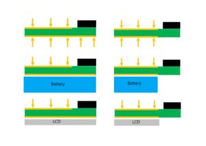
Figure 2 shows the two forms of ground plane in yellow, with the PCB is shown in green, and the antenna component in black.
NB-IoT products are an interesting area of development right now, with many new applications in remote-controlled lighting, tracking and wearable electronics. However, the greatest demand is for smaller products, which means the devices must work with shorter ground planes and cannot use too much power.
This presents a dilemma for the designer, because for antennas to operate at sub-1GHz frequencies, they need ground plane lengths of 100mm or more to prevent antenna efficiency from dropping. If the antenna efficiency should drop, this will cause issues gaining network approval for the finished product. So, the challenge for the product designer is to create a physical design that meets the limitations of size and space, and still performs well in operation.
Consideration for how the antenna and pcb are incorporated into the overall design may take advantage of being attached to either a wiring harness and plug such as in OBD2 devices or connecting to a larger device through data I/O and power buses extending the electrical ground plane presented to the antenna.
Efficiency
Efficiency is the single most important measure of antenna performance. It describes the portion of radiated power which is supplied to and radiates away from the antenna. In small, battery-powered devices, achieving efficient performance is integral to the longevity of the device.
There are plenty of factors to consider when examining potential areas to improve antenna efficiency. Some of these include:
- Resonant frequency shifts caused by reflective or absorptive masses placed near the antenna.
- Metallic casing or glass filled nylon plastic housings near or around an antenna, which will cause a null or depression in the 3D radiated pattern inhibiting radiation in the direction of the null.
- Nearby antennas with similar frequencies which may detune one another’s near-fields. We recommend that they should be isolated up to -10dB <1GHz and -20dB for 2GHz as a minimum
RF Modules
Like SMD antennas, modules are complete antenna solutions which can be placed directly on the pcb. The advantage these have over standard surface-mounted antennas is that they come pre-assembled. The antenna will already have a chip and other key components.
These work well for GNSS applications. They effectively offer a ‘drop-in’ solution, which means that designers do not need to spend time designing in complex RF circuitry.
Outer casing
Having considered the antenna’s position on the pcb, it is also important to think about the outer casing for the device. Metal is not conducive to effective antenna performance. Conductive surfaces become charged when in contact with electromagnetic fields and become radiators. This causes a range of issues for effective antenna performance.
It is also important to consider the gap between the casing or housing and the antenna. Plastic has a higher dielectric constant than air, so placing an antenna too close to a plastic cover is also likely to detune the signals.
Tips for antenna integration
Some tips for successful integration of a chip antenna:
- Select an appropriate ground plane length for the lowest frequency of the antenna.
- If the antenna is ground plane free, make sure that all the pcb layers under the antenna are free, and that no metallic objects such as a battery or LCD are placed beneath it.
- Never run digital traces underneath the antenna or wires above/below it.
- Respect the ground plane clearance shown in the datasheet.
- Never use narrow traces or unnecessarily long transmission lines.
- Some antennas need to be placed in the pcb corner, whilst others are to be placed along the long edge of the pcb; find an antenna which integrates seamlessly within your design.
- Do not place large or noisy high-speed switching components nearby.
The authors are Geoff Schulteis, senior antenna applications engineer and Robert Dumont, America’s sales manager, Antenova Ltd. – www.antenova.com