How T&M addresses the coming 6th wave of innovation
By Wilson Lee, Technical Marketing Manager, Tektronix Inc.
Electronics Test & Measurement Supply Chain applications connected connected intelligence measurement measurement test testThe new world we’re entering into is centered around connected intelligence with new devices, new applications, new business models and new services emerging all around us.
The Russian economist Nikolai Kondratiev first recognized the concept of major waves of innovation in 1925. The five initial major economic waves have since been defined as the industrial revolution; the age of steam and railways; the age of steel and electricity; the age of oil, cars and mass production, and the age of information and communication. Each wave ranged from 40 to 60 years and consisted of alternating periods between high sector growth and periods of slow growth.
In 2010, Dr. James Bradfield Moody authored The Sixth Wave where he postulated that we are on the cusp of a sixth wave that will be defined by resource efficiency. He theorized that this new wave would be heralded by massive changes in the market, societal institutions and technology that all reinforce each other. These include rising scarcity of ore grades, increase in water demand, and an increasing recognition of the economic value of efficiency. In the ensuing years, the sixth wave hasn’t exactly materialized the way Moody envisioned, but the basic premise that we’re entering a sixth wave is spot on, even if it won’t be centered solely on resource efficiency (even though that is an important component). The new world we’re entering into is centered around connected intelligence with new devices, new applications, new business models and new services emerging all around us.
At the center of this world is the internet of things (IoT). For this discussion, the IoT could be more aptly named the intelligence of things which is being driven by two powerful elements: the sensorization of things and the digitization of things. Already we’re seeing millions of tiny sensors tracking and monitoring everything from the steps we take and the calories we burn to our home’s energy consumption. Sensors are present in phones, parking meters, streetlights, on factory floors in manufacturing equipment, automobiles, wearables and even in golf balls. The sensorization and connection of things represents a powerful wave of innovation.

Connected intelligence will power the coming sixth way for innovation.
The second driver in the sixth wave is the digitization of things. The digitization of things has been taking shape for years. For anyone with a teenager, you only need to watch them interact with their cell phones for a few minutes to understand the amount of digital data they produce and consume. Digital data is a fabric of their existence. In the business world and in many government organizations, more and more leaders are concluding that there is tremendous value — financial, productivity and competitive — in the massive volumes of data being collected. And this data will be analyzed using artificial intelligence to derive game-changing insights to drive further innovation. This will in turn lead an acceleration in the pace of change.
This isn’t to say there aren’t challenges in delivering on the promises of connected intelligence. One of the biggest could be the so-called interference of things, which can take many shapes and disrupt the flow of data. This includes noise, such as EMI/EMC interference from multiple devices in the same shared spectrum. Indeed, making sure all the many components and systems behind connected intelligence operate smoothly together represents a complex test and measurement challenge, and it will likely be many years before they are fully overcome.
As the connected, intelligence economies unfold, there will start to be a blurring of industries and many of the long-established domain boundaries will start to disappear. Automobiles designers, for example, now must be experts at power management, know how to integrate mobiles apps and be capable of managing massive data streams. With this in mind, you can see why internet search companies are now moving into driverless cars. This type of movement creates new opportunities, but also new risks as new players or market contenders emerge.
Just as the sixth wave promises profound societal change, it similarly has profound implications for many industries, not the least of which is electronics design, test and manufacturing. Arguably, the industry has never seen such pervasive, across-the-board changes like what we’re seeing today. The pressures facing designers to deliver significant innovations in shrinking time windows is unprecedented. To be successful, designers must begin to view test and measurement as an innovation platform rather than a hurdle to be overcome. Let’s take a closer look at how the challenges facing engineers, and the role of test are changing in a number of industry segments.
Connected Car
Multiple technologies and systems are coming together to create connected cars, including communication technologies such as Wi-Fi, Bluetooth, Zigbee, 5G and 100BASET-T1 and more. Environmental testing is critical to account for the interference of things generated by these multiple RF sources. Greater integration between subsystems is driving fundamental architectural changes that require new strategies as the industry moves from isolated systems to networked systems, including gateways connected to a backbone. Subsystems are generating massive data which has to be moved rapidly and without errors throughout the car.
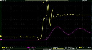
These increased speeds and associated complexity mean that automotive engineers will have to learn new tools and techniques and move to higher-performance test instrumentation. It’s important, however, for test and measurement suppliers to reduce the inherent complexity involved, bring solutions which are more integrated, and shorten the time to insight. Automated tests, such as the Power Spectral Density test shown, below give designers a way to easily confirm compliance with standards by comparing results to test limits.

Automated tests, such as this Power Spectral Density test, give designers an easy way to confirm compliance with standards by comparing results to test limits.
Power Management
The engineering and testing challenges brought on by the IoT are immense. Engineers must figure out how to squeeze more efficiency out of these new devices, and more importantly how to actually test and validate that designs will work in the real world. The need for high efficiencies and small form factors in power designs is pushing engineers to use higher and higher switching frequencies and smaller component packages. This has led to the development and use of new wide bandgap switching technologies such as gallium nitride (GaN) and silicon carbide (SiC) which can switch significantly faster than traditional silicon devices and deliver significantly more power per square millimeter.
The need for testing and evaluating at the component level also increases significantly when deploying new technology such as GaN and SiC. The devices need to be tested for breakdown up to thousands of volts and at the same time vetted for leakage currents that can be as low as femto-amps. Robust testing of these devices, all the way from wafer to the package parts, becomes critical given the demanding designs in which they are deployed.
A particular challenge has been testing on power devices with fast switching rates in the presence of common mode voltage as conventional differential probes derate over frequency. This has led to the development of optical probes to overcome these limitations and allow accurate characterization of high-side devices, as shown below.
New probing solutions can reveal details of what is occurring in a design that were previously hidden.
At the system level, the need for extremely high efficiencies requires the evaluation of smaller incremental design changes. This game of nanowatts requires very precise measurements over all operating modes. For example, current draw during deep sleep modes and transmit modes can require several decades of measurement range with a fast measurement rate to capture the details.
Datacenter/Wired Communications
With the rapid proliferation of connected devices and sensors, we’re dealing with more data than ever before and that is driving the need for faster bandwidth within and outside of datacenters. The data must be stored and accessed quickly and reliably. Exponential increases in data volumes are driving new technologies across the ecosystem and must be balanced with the need to keep everything low-cost and low-power.
The interplay of new standards, approaches, and technologies makes measurement more important than ever. Design complexities are a lot greater than what they were in the past, and engineers will need to run more tests to make sure that a product is solid. As technology becomes more complex, there will be new challenges in interoperability and a greater focus on making sure components work together in specific applications.
Military/Government
When people think of aerospace and defense, most of the attention focuses on applications like RF sensing, satellite communications and electronic warfare, which are of course critically important. But when you a look a little closer you’ll see that there’s far more than just those applications going on. Intelligent, connected devices are having a big impact and are now being used to connect aircraft, machines, systems, and people in aerospace and defense systems for improved performance and lower total operating costs. Recent reports indicate that this is now more than a $20 billion market alone. Taken as a whole, test and measurement plays a critical role in enabling innovation in this industry, offers equipment that enables greater insight as shown below, accurately recreating threat environments or helping military system overcome the interference of things.
New equipment enables greater insight into RF environment enabling engineers to see things that were previously invisible.
3D Sensing
3D sensing is a depth sensing technology that augments camera capabilities for facial and object recognition in augmented reality, gaming, autonomous driving and a wide range of applications. The adoption of 3D sensing for smartphones is driving down size, power and cost — it must fit in a handset and use minimal battery power– while driving up performance. This is also enabling expanded use of 3D sensing in other end applications such as automotive and industrial robotics. The need to test all of these applications is critical as they all have a safety or security component to them.
As we enter the sixth wave of innovation, one of the factors that will distinguish winning organizations is speed. In the hectic and rapidly changing environment that lies ahead, speed is a weapon in the hands of engineers as they try to commercialize technology. The engineering teams who bring innovative new technologies to market faster than their competitors, and who are able to cross established boundaries, will ultimately emerge as the winners.
# # #
About the Author
Wilson Lee is Technical Marketing Manager at Tektronix. He has over 25 years of technical marketing, technical sales leadership roles with manufacturers such as CTS Electronic Components, as well technical/value-add distributors such as Richardson RFPD and Premier Farnell. Wilson has focused heavily on design and design engineer engagement within the RF/Wireless, Industrial Power, and Industrial Automation market segments. He holds a Bachelor of Science from Cornell University.