The role of solderability testing
By Reid Henry, president, Hentec Industries/RPS Automation
Electronics Production / Materials Editor Pick equipment productionIts importance in successful soldering
One frequently asked question is what is solderability testing and what function does it perform. Solderability testing is not component preconditioning but is a measure of the ease with which a solder joint can be formed. Solderability testing is used to assess the solderability of device package terminations and varies depending on the type of solder alloy used. For example, when using various lead-free alloys, solderability can differ significantly from solderability when using lead-based solder.
Background
In 1983 the US Department of Defense (DoD) determined that over 40% of military electronics system field failures were electrical in nature and some 50% of these failures were due to poor solder connections. Plated finishes, usually nickel (Ni) or tin (Sn), were found to be porous and non-intermetallic allowing oxide penetration to the base metal which led to poor solder joint integrity and therefore resulted in field failures. As a result, the MIL-STD-883 solderability testing standard was instituted to assure that all components in high-reliability applications were indeed solderable and plated finishes gave way in favor of a hot solder dip finish performed by the robotic hot solder dip process which provides a fused tin-lead (SnPb) homogeneous surface finish to enhance overall solderability.
Solderability test methods
The MIL-STD-883 Method 2003 is one of the oldest and most widely used standards for solderability testing within the electronics assembly industry. It is used as the basis for the following discussion to provide details on how solderability testing is normally performed. The MIL-STD-883 standard employs the dip-and-look solderability method, requiring the following equipment: 1) a solder pot of sufficient volume that can maintain solder at a specified temperature, 2) steam aging equipment for aging of the samples prior to testing, 3) a dipping mechanism capable of controlling the rates of immersion and exit speed, as well as dwell time, of the terminations, and 4) an optical inspection and lighting system that facilitates a minimum of at least 10X magnification.
Why perform test solderability?
Solderability testing provides a means of determining the solderability of device package terminations that are intended to be joined to another solderable surface using either tin-lead (SnPb) or lead-free solder alloys. The reason for performing solderabilty testing is to detemine if a component provides the degree of wetting necessary to form a robust solder connection. A poor solderabilty test result indicates that a less-than-optimal connection could be formed. Solderability testing is also effective during various aspects of printed circuit board production, such as when evaluating different printed circuit board coatings, various solder alloys, solder paste, or flux materials.
In addition to today’s consumer driven electronics marketplace, there are many industries that require semiconductor devices to have a longer lifecycle such as the industrial, automotive, medical, aerospace and defense sectors which dictates long-term component storage. Whenever long-term storage is required it is critical to ensure electronic components are reliable with a key measure of their quaility being solderability testing.
Testing protocols
Solderability testing is designed to determine how well molten solder will wet on solderable surfaces. Most common categories of solderability testing are qualitative testing and quantitative testing. The most common qualitative testing method is the dip-and-look method which involves subjective examination via comparative analysis of test samples. The most common quantitative testing method is the wetting balance method that requires interpretation of a wetting balance curve.
The wetting balance test is used to measure the wetting forces between molten solder and the surfaces of a test specimen as a function of time. Solderable surfaces differ in speed and strength of adhesion therefore the wetting balance test measures the time for various solder alloys to wet a components terminations or pads.
The dip-and-look test is a method in which a test specimen is completely immersed in molten solder and then visually inspected. The test piece is dipped into a molten solder bath, usually by an operator. The component surfaces to be wetted are first wetted with flux and then completely immersed in a molten solder bath followed by visual examination (Figure 1).
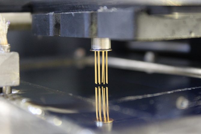
Figure 1: Test specimen dipped in molten solder bath during dip-and-look solderability testing protocol.
The most prevalent suppliers of dip-and-look solderability test equipment are Cemco (UK) and Hentec/RPS (USA), while the major wetting balance test equipment suppliers include GEN3 Systems (UK), Malcom/Seika (Japan), Metronelec/Quiptech (Germany), Microtronic (Germany) and RHESCN (Japan) along with other minor suppliers.
In addition to aging of samples prior to solderability testing, steam aging equipment can also be used for accelerated life testing to simulate elongated storage conditions of surface mount or through-hole components. If additional testing is required for mission critical applications, X-ray fluorescence (XRF) can be used to measure the solder thickness of the component terminations and scanning electron microscopy (SEM) can be employed to probe the intermetallic layer if necessary.
Acceptance criterion
The main acceptable criterion for solderability testing as defined by the MIL-STD-883 Method 2003 standard is 95% coverage of the dipped portion of the terminations with a new and continuous solder coating. Therefore, pinholes, voids, porosity, non-wetting, or de-wetting must not exceed 5% of the total dipped area of the terminations. Besides the MIL-STD-883 Method 2003 standard, other common solderability test standards include the IPC J-STD-002 standard. Other solderability test standards include MIL-STD-202 Method 208, J-STD-001 Space Addendum, J-STD-001ES, J-STD-003, JEDEC JESD22-B102 and MIL-STD-750 Method 2026.
Qualitative vs. Quantitative
Solderability testing determines how well molten solder will wet on solderable surfaces of electronic components with the most common solderability test methods being the dip-and-look method and the wetting balance method. The dip-and-look method is a qualitative type test performed by comparative analysis after specimens are dipped in a bath of flux and molten solder. The wetting balance method is a quantitative type test based upon the interpretation of a wetting curve measuring the buoyancy of a specimen using a load cell. There are several solderability test standards, but the most common standards are MIL-STD-883 Method 2003, IPC J-STD-002 and MIL-STD-202 Method 208.
While the wetting balance test method is precise and measures the wetting forces between molten solder and a test specimen as a function of time, it requires the interpretation of a wetting curve by skilled personnel in a laboratory environment. Another disadvantage is that wetting curves can be easily distorted if the system is not properly calibrated or if a wetting balance test is performed incorrectly by unskilled, or inadequately trained personnel.
An advantage of the dip-and-look method is since it is based on comparative analysis it can be performed rapidly by shop floor personnel with minimal training as well as requiring significantly lower capital investment then a wetting balance test system which is considerably more expensive. An additional advantage of the Hentec/RPS Pulsar dip-and-look test system is it can also be configured for low-volume lead tinning of component terminations that exhibit poor solderability due to excessive oxidation or prolonged storage (Figure 2).
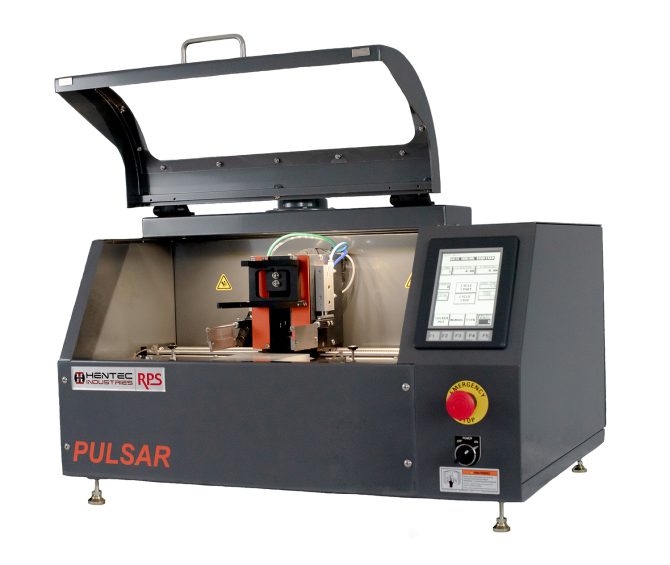
Figure 2: Hentec/RPS Pulsar dip-and-look solderability test system designed to meet IPC J-STD-002 requirements.
For some high-reliability applications additional solderability testing may be required and can include steam aging which is used for accelerated life testing to simulate elongated storage conditions. The Hentec/RPS Photon steam aging system is designed to generate artificial aging simulating elongated storage conditions of electronic components and is especially suited for high-reliability applications or end-of-life product builds (Figure 3).
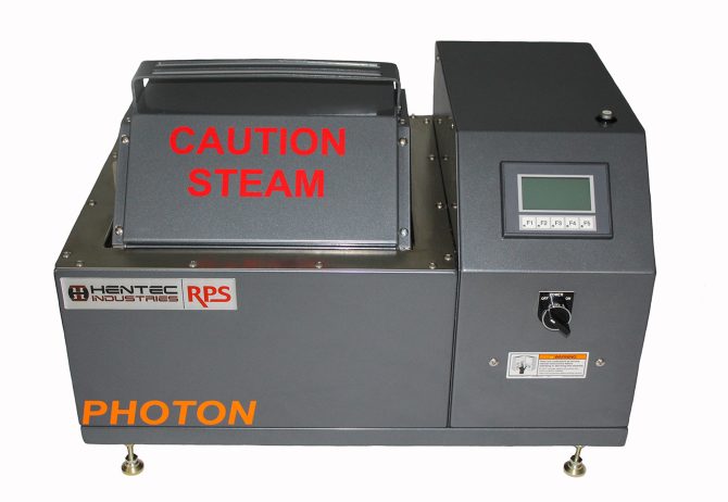
Figure 3: Hentec/RPS Photon component steam aging system designed for accelerated life testing simulating elongated storage.
The Hentec/RPS Photon steam aging system is multi-purpose as it can perform both aging of samples prior to solderability testing, as well as simulating elongated storage conditions of surface mount or through-hole components and accelerated life testing.
Solderability test procedure
The general solderability test procedure as noted by the MIL-STD-883 Method 2003 standard consists of the following steps: 1) proper preparation of the samples as defined by an acquisition document, but which must not include wiping, cleaning, scraping, or abrasive cleaning of the terminations to be tested, 2) aging of the samples in a steam ager, which consists of exposing the surfaces to be tested to water vapor for eight (8) hours and drying them either by baking at 100ºC for no more than one (1) hour in a dry atmosphere or air drying them at ambient temperature for a minimum of fifteen (15) minutes; 3) proper application of flux to the terminations; 4) solder dipping, which consists of immersing the terminations in a static solder bath at a uniform temperature of 245C ±5ºC; followed by 5) examination of the terminations at 10-15X magnification.
Summary
Solderability testing is essential to ensure that robust and reliable solder joints are formed for most electronic packaging and circuit board assembly applications. Solderability should no longer be consider as an option for many high reliability segments of the global electronics assembly industry, particularly whenever long-term component storage is involved. Therefore, to ensure product quality solderability testing is a highly recommended component testing protocol.
——————————————
Hentec Industries/RPS Automation designs and manufactures a complete line of high precision selective soldering, lead tinning, and solderability test machines.