Prototyping for the Internet of Everything
By JF Brandon, sales & marketing, Bot Factory
Automation / Robotics Electronics Production / Materials Engineering IoT Printable Electronics Supply Chain 3D 3D internet of everything IoT printed electronics printed electronics prototyping prototyping3D Printed Electronics helps deal with the Explosion in IoT Applications
Electronics have completely enveloped our daily life – from cradle to grave we are connected to and wholly reliant on electronic devices. The promise of the future is that every object – no matter how banal – can become smart. However this promise is hamstrung by the difficulties of prototyping a potential idea and getting it to market. There are already existing means to prototype printed circuit boards (pcbs) today, but advances in 3D Printed Electronics (3DPE) offer a wider range of design possibilities to the engineer at a quicker turnaround time for a lower cost.
SV2 printed circuit board printer from BotFactory.
For entrepreneurs, the IoT boom has opened up possibilities of creating new products in existing markets. In 2014 a trio of smart air conditioning (AC) startups – tado, Sensibo and Ambi Labs collectively raised $500,000 in crowdfunding campaigns for their respective products. Existing businesses have stepped up to retool their own product line, re-configuring their products to become smart to protect and grow their market share. HVAC heavyweight GE Appliances recently released their own smart ACs. Edison famously said that Invention is 1% inspiration and 99% perspiration – would a smarter Air Condition cool an overworked and vexed inventor better than before?
Prototyping and pushing out products quicker often means gaining the initiative over the competition – provided the product works well. One month saved on product development is one more month in the market selling to customers. For startups with a big vision, or a Fortune 500 with a big budget, delivering on time is critical – and prototyping quickly is key.
Unprecedented demand for rapid prototyping
UK-based Market research firm IDTechEx specializes in studying this problem. “Due to the proliferation of ’ubiquitous computing’,” states IDTechEx director Dr. Jon Harrop, “there is unprecedented demand for rapid prototyping of low-power electronic circuit boards.”
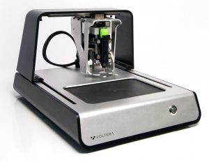
Voltera V-One desktop printed circuit board printer.
For decades, the most common techniques for prototyping pcbs was milling, in-house etching or quick-turn, third-party vendors. Creating anything more than a rigid two layer board required something equivalent to a pcb fabrication line, so overwhelmingly companies have relied on quick-turn third-party vendors. Often based in Asia, these vendors pool orders into one production run to reduce cost at the expense of time – 24 hour runs increase costs by 5x to 10x. Exotic requirements like metal-core or flexible substrates drive prototyping costs even higher.
To address the fundamental issues with third-party vendors, engineers have turned to a new kid on the block – 3D Printed Electronics – for their prototyping needs. “3DPE is already starting to fill that gap in the market.” Harrop says. But is it better than existing tools at hand? “CNC milling is the next best technology after 3DPE because it can be done on the desktop and can even support high power circuits but it is messier, less reliable and effectively limited to two-layers compared to 3DPE.”
Eliminating costs of unavoidable design change
The mess can be exported to third-party vendors, but according to IDTechEx’ market research, circuit designers do pay for existing off-site pcb fabrications, but it turns around and ravages research budgets when an unavoidable design change is needed, or unexpected problems crop up.
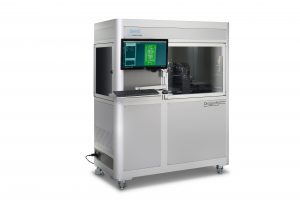
DragonFly 2020 Pro 3D Printer from NanoDimension
“So 3DPE has a promising future as the first reliable and clean desktop solution for quick-turnaround circuit prototyping,” according to a IDTechEx report.
Israeli-based Nano Dimension Ltd. is one company in the thick of this movement, leveraging new developments in nanoparticle silver inks and ink jetting techniques to create high density, multilayer circuitry. Their Dragonfly Pro 3D Printer is capable of creating 8 layer boards in less than 12 hours, printing traces as thin as 5 mil (125 micron), but with a price tag above CND$260K their typical client is institutional or multinational.
On the other end of the spectrum, Waterloo-based Voltera has focused on dispensing its own nano-silver pastes via dispensing, creating two-layer boards using a new drilling function. The Voltera V-One can create rigid or flexible circuits by these means at a much quicker speed than milling or etching at a price of $3,500.
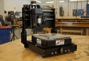
Between the two ends is NYC-based BotFactory and its new $16,000 SV2 PCB Printer, which utilizes a single frame with multiple, hot-swappable heads for inkjet printing, paste dispensing and even pick-and-place. Capable of 8 mil (200 micron) traces and more than 2 layers, the SV2 was designed as a complete, all-in-one tool for electrical engineers, researchers, teachers and students.
The common thread with additive manufacturing of pcbs is the use of nanoparticle silver. Generally speaking, when a metal is refined to the nanoscale particle size it can sinter and melt at temperatures well below their bulk melting points. Off-the-shelf Ag inks and pastes often sinter below 100C in atmosphere conditions, and exhibit conductivities close to that of bulk silver. Combined with polymer inks (as with BotFactory and NanoDimensions), it is possible to create boards with as many layers as one wants, and do novel things such as buried or blind vias without any added costs. As with all AM technologies, complexity is free.
Electronic 3D Printer is a powerful tool
For the electrical engineer, having an electronic 3D printer is a powerful tool for experimenting in new areas such as flexible electronics without walking the tightrope of sending boards out for prototyping or using basic in-house methods such as CNC milling. According to a recent survey of pcb designers and electrical engineers carried out by Nano Dimension Ltd., 3D printed electronics is expected to become a commonplace tool for them. The survey showed that more than three quarters (76%) are already exploring the technology for design validation (31%), prototyping (40%) and low-volume custom manufacturing (29%).”, with 85% stating that accelerating product development was their primary concern.
Having an all-in-one solution for fabricating and assembling any type of pcb was the ultimate goal for BotFactory because its goal has been to make hardware engineering ‘agile’ like software development has become. By organizing electrical problems via ‘scrums’ and creating new boards in an iterative manner, the path to market becomes relatively straightforward. By condensing all the processes of a typical pcb factory into a desktop package, the ultimate cost to a business is reduced both from time saved and prototyping fees.
Considering how much the electronics industry focuses on miniaturization, it only seems logical that the pcb factory become finally shrunk into something a little more manageable.