The pcb design ecosystem
By John McMillan, Mentor Graphics Corp.
Embedded Systems Engineering John McMillan Mentor Graphics Corp. pcb designAccess to design IP and collaboration is key to meeting the needs of engineers in electronics product design.
In printed circuit board (pcb) design, a product creation ecosystem enables engineers to address the nuances of design early and throughout the technology development cycle. From component selection to manufacturing output, a robust, scalable, and unified pcb design tool is needed to meet critical performance, schedule deadlines, and cost challenges.
Collaboration within the pcb design ecosystem.
Yes, today’s high-tech products are faster, smaller, and smarter than ever and the time-to-market demands to deliver high-quality products that are competitive, cheaper, and faster means that design tools must be able to consider every aspect of the design throughout a product’s creation, from functional specification to end-product performance. And with IoT, Bluetooth, WiFi, and RF technologies everywhere, design concerns related to mixed signals, power consumption, and thermal analysis must be measured and addressed throughout every stage of the design, from the component level through to final assembly.
Unified tools
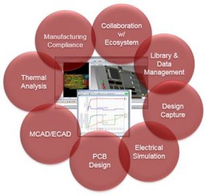
Managing the pcb design ecosystem from within a unified design tool enables engineers and pcb designers to leverage design IP with the final product in mind, analyzing and validating each aspect, effect, and impact encountered along the way. From part selection, design reuse, simulation, and early collaboration with MCAD, the design ecosystem can ensure end-product success.
Collaboration within the pcb design ecosystem
From the earliest stages of component selection, each critical parameter must be considered. Access to qualified components and component and symbol management are key within the ecosystem. Library databases must be kept in sync and up-to-date to ensure that availability, manufacturability and inconsistency issues are avoided.
Having a single, integrated, centralized library, access to a qualified component portal for research and supply of qualified library symbols, and a built-in synchronization mechanism that alerts you and makes necessary updates whenever a database mismatch occurs, are critical to creating and maintaining the component library in the ecosystem.
Constraints drive component placement and routing. From differential pairs to clock signals to transmit-and-receive lines, trace spacing and length rules must be understood, applied, and adhered to. A design ecosystem that ensures constraints are maintained and stay synchronized through each step of the pcb design flow is essential.
Today, most pcbs have multiple FPGAs and more than 90% of nets have high-speed constraints. In the pcb ecosystem the importance of a unified constraint management system that spans both schematic and layout environments ensures that design integrity is implemented, applied, and maintained throughout the design process.
Ability to analyze and simulate power rails
Engineers also need to quickly assess voltage-drop issues of power delivery networks (PDNs). The ability to analyze and simulate power rails for FPGAs, ASICs, and other components with tight tolerances throughout the pcb layout phase and within the design ecosystem, ensures clean power and reference voltage to active devices and prevents malfunctions or failures due to excessive voltage loss.
Thermal analysis is another important design element in the ecosystem. By exploring and accurately simulating the design space, pcb designers can consider the effects of all aspects of the design, including package selection, pcb layout, board structure, and the enclosure, to ensure that the most cost-effective cooling solution is chosen.
To be a true ecosystem, there must be collaboration between ECAD and MCAD. Communicating design intent between electrical and mechanical CAD systems through true, real-time MCAD collaboration enables designers and engineers to import and collaborate on exact 3D models of the board outline, mechanical enclosure, mechanical components, and even other pcb mezzanine or daughter cards at any time throughout the design process.
Though often thought of as a post-design process, design checks are an important part of the pcb design ecosystem that should be considered throughout the design flow. Design rule checks (DRC) and design for fabrication checks not only ensure that product performance is optimized, but that design integrity is not compromised during fabrication. With built-in features like DFT (Design for Test), DFM (Design for Manufacturability) and DFA (Design for Assembly), you can ensure the lowest possible product cost, the fastest possible process cycle time, and the highest possible first-pass yield.
Putting it all together
Designing within the pcb design ecosystem on a single platform ensures that designs are robust, reliable, and can achieve first-pass design success which results in meeting tight schedules by eliminating re-spins and keeping costs low. Pcb design tools that support an ecosystem approach also enable designers and engineers to address every aspect of product creation from beginning to end. From system simulation to design capture through to layout, DFM analysis, design archiving, and collaboration between and with each technology area of pcb design, PADS electronics product creation platform delivers a powerful and scalable ecosystem that enables individual engineers, designers, and small teams to design, lay out, and validate high-quality products, from concept to reality.