Lost in transmission: Solving common issues in high-speed design
By EMA Design Automation Inc.
Electronics Engineering Software Engineering pcb design pcb design software softwareCreating a printed circuit board with high-speed design functionality is no small feat. The more complex a PCB design becomes, the higher the chances are of running into high-speed PCB design issues.
Often, high-speed design problems will present themselves in specific ways that, to the untrained eye, may not be so obvious to diagnose. These issues can result in late-stage changes, delivery issues, and unpredictable costs to your board. Here, our experts at EMA will provide the tips and tricks you need to achieve high-speed design success.

What is High-Speed Design?
As today’s technology becomes more complex, so do the circuit boards required to handle it. The basic concept of creating a circuit board is to place your components in a layout where they can “talk” to each other using signals. When a PCB has many physical components, these signals can easily become garbled. The level of measured integrity to the signals is what we define as high-speed design.
Technically speaking, when the path delay of a signal is long, compared to the rise-time of the conducted signal, it’s considered high-speed. Practically every design today has some aspect of high-speed behavior involved, which is why, as a PCB Design Engineer, it is more important than ever to be able to diagnose and correct the issues the signals may present.
Hint: It’s More Than Just Time
When you find issues late in the design cycle, it can severely impact your project. Today’s design requirements and time-to-market demands don’t allow for open-ended build schedules. Therefore, it is extremely important to find problems as early as possible. Doing so will prevent increased manufacturing costs, re-spins, missed schedules, and the ripple effect from project delays. 
Not only will you save time and money, you will also find a smoother workflow overall. Identifying and resolving your high-speed design issues will ultimately allow you and your team to move through to the layout and manufacturing stages faster, with fewer errors to be fixed in each round. A faster process will result in increased overall production value, and ultimately aid in the growth of your product.
You cannot fix what you do not know is broken. One of the key challenges is being able to identify high-speed design issues in the first place. To help, we will delve a bit deeper into the common root causes of high-speed design issues: noise and timing.
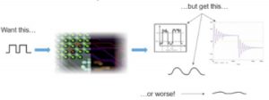
The first problem many designers face is signal noise. Considered to be anything undesired or not intended, signal noise is often detected as anything “extra” in your signal waves that degrade the quality. Digital signals ultimately need to be defined as ones and zeros, so when there are extra bits, the clarity is confused and muddy. Additionally, signal noise also promotes electro-magnetic radiation (EMI) effects. Such affects will damage signal integrity with emissions and crosstalk.
Most noise issues can be attributed to any combination of three subject areas: impedance mismatches, coupling issues between adjacent “fast” signals, and return-path discontinuities. Each has its own impact on the project and several possible solutions to fix it.
Impedance Mismatches
Issue: Impedance values are not consistent.
Impact: Consistent impedance is very important for signal quality. Each segmented entity within a signal trace can have drastic changes in impedance values and, if not consistent, cause a variety of problems. Symptoms may manifest as signal ringing, delays associated with overshoot and undershoot, and reflections that reduce signal quality. Impedance mismatching can also affect the timing of your signals. When a signal must overcome a specified amount of delay, it will impact your timing margin.
Fix: There are several ways to correct the mismatches. First, locate and move problematic segments. You may also need to resize the trace widths or alter the stack-up directions. These solutions are easy to manage early in the design cycle but become costly if the design has progressed too far.
Coupling Errors
Issue: The proximity of two signal traces to one another.
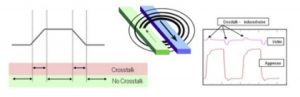
Impact: Coupling issues are a function of signal “edge” speed and the proximity of each signal trace to one another. Most issues occur within the rise and fall rates of your signal transmissions. Fast signals are the aggressors and can victimize any adjacent trace. Long parallel runs are the easiest victims and will cause false switching points and unwanted noise. The stack-up can also affect coupling issues in cases of thicker dielectric layers and different materials than the norm.
Fix: If the trace-to-trace spacing is too narrow, you must move one of the traces. With too long of a parallel routing length, disrupt the parallelism. In stack-up cases, you may need to alter the stack-up. Lastly, when the signal edges are too fast for the board design techniques, slow down the signal edges where possible. Many of these issues will also have costly fixes when found in later stages of the design and/or manufacturing process.
Return-Path Delay
Issue: Discontinuities in a return path.
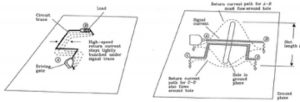
Impact: Important for good signal quality, discontinuities can affect trace impedance and cause delay. Signal currents will use the path of least resistance to return to the source, so issues such as split planes will create gaps and return path discontinuities, degrading the signal and diminishing the quality. These complications in turn prevent smooth current flow and effectively lengthen the return path. Additionally, they will generate unwanted radiated signal emission from your board (EMI).
Fix: In simple cases, you may add more reference planes. The best option would be to move power and ground planes around to avoid breaks under the signal paths. Alter the signal paths to avoid discontinuities and create a smooth flow.
Getting There in Time
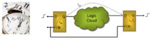
The second, most common high-speed design issue is timing— every signal needs to arrive at its destination within some specified time frame. Typical timing requirements involve times for signal arrival, signal remaining stable, and signal state to be recognized. When one or more of these requirements are not met, your timing may fail.
Successful signal timing is imperative to a working board. With timing, the impact of the issues is more straightforward to describe. In all cases, the signal is simply not arriving at its destination when it is expected to. The causes of bad timing can be broken down into several categories: phase mismatching, propagation delays (both total and relative), impedance mismatching, rise and fall time distortions, and threshold crossing distortions.
Solving the impedance-related problems should be a top priority, as they are a primary cause of timing issues. Minimizing them may result in board alterations, so it is important to catch these errors as early in the process as possible. Next, make sure to measure the entire delay path for accumulated delay, which can often require taking pin and z-axis delays into account. Lastly, resolve any phase issues with differential clocking signals, as these can lead to severe timing problems by distorting reference clocks.
Rules of Thumb Are No Guarantee
In PCB design, many designers employ a set of Rule-of-Thumb guidelines. These can be a good starting point in your design but are ultimately not a guarantee to find related problems. When you lay out your board, a rule of thumb does not give feedback or a good vision of how your board will perform under conditions of impedance, coupling, return-path reference, or signal timing. Therefore, there is a need for a more conclusive analysis system during the design cycle.
Design cycles have many steps, and when problems occur early on, they are often compounded through to the end and result in costly re-spins. When critical decisions need to be changed late in the process, it can have a ripple effect throughout the design. Having a working high-speed design management system in place will ensure a smooth process with minimal delays.
Real-Time Design is a Safe Bet
Wouldn’t it be better to identify potential problems you’re dealing with early in the design cycle? Avoid the ripple effect of errors with Cadence Real-Time Design. Control and manage your designs in real-time, with system checks that will flag violations to be fixed before you send it on. Catching and correcting high-speed design issues early in the cycle means a highly streamlined design release process that will vastly improve your time-to-market schedules. Eliminate multiple validation iterations and boost your productivity with Real-Time Design.