How to add RF and lower compliance costs
By Rich Markley, product manager, Rohde & Schwarz’s Value Instruments
Electronics Test & Measurement EngineeringIt’s almost oxymoronic, but it’s possible to add RF capability and lower compliance costs by following some basic steps.
With more devices requiring radios, EMI and EMC increase in importance, particularly as designs move to faster clock speeds, smaller form factors, lower power rails and more data lines. However, the combination of power supplies, sensitive electronic circuits and RF components increases the potential for costly compliance test failures, which are already at 90 percent for first-time tests.
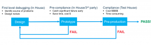
Figure 1: Catching EMC issues early in the design cycle can decrease the cost of compliance testing.
To speed time to market and lower risk, designers need to do pre-compliance testing of their devices to increase the odds of passing the formal compliance test. This testing and associated debugging can be done using relatively low-cost spectrum analyzers and oscilloscopes.
This assumes a solid understanding of the equipment under test (EUT) and that some core best practices are followed.
The need for pre-compliance testing
Compliance testing to one or more specifications, as defined by the FCC, CISPR, CE or other bodies, is standard practice to ensure devices do not interfere with nearby equipment and that they are not susceptible to external interferers. However, the Internet of things (IoT) and subsequent technologies such as machine learning and artificial intelligence (AI) have resulted in the proliferation of RF technologies to gather data.
As many designers quickly find out, incorporating RF is not easy. Custom designs usually take longer than expected, and while RF modules are an easier route, they too come with added complexity of circuits that both cause and are susceptible to on-board and external EMI. This adds to the many other potential sources of EMI problems, such as power supply and LCD emissions, ground impedance, poor cable shielding, stray internal coupling paths, component parasitics and ESD in metallized enclosures.
All these factors contribute to increasing the odds of a device failing formal compliance testing, which adds time and cost (Figure 1). Studies put first-time failure rates at 90 percent. This failure comes at high cost, as over-the-air and conductive testing with a third-party test house can cost $10,000, or more, and takes place over a number of days.
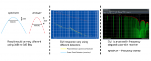
Figure 2: In receive mode, spectrum analyzers imitate higher cost EMI receivers and can be used for pre-compliance testing.
The goal from the designer’s point of view is to decrease the odds of compliance test failure to the point of only needing to do this test once. This is where pre-compliance testing comes in.
Pre compliance testing using standard equipment
There are two main reasons that designers don’t do pre-compliance testing. The first is that they don’t think it’s worth it, given the time-to-market windows and delivery schedules. The second is that they think it requires expensive EMI receivers. Both can be addressed using a standard, low-cost spectrum analyzer, an ably-equipped oscilloscope, and some EMI test and debug best practices. While the EMI receivers cannot be completely replaced by a lower cost spectrum analyzer, the lower cost approach can do the work of some of the EMI compliance functions and help to identify potential problem areas before discovering these later in the EMI compliance lab.
To perform pre-compliance testing, the first challenge is to isolate the device under test from ambient RF interferers, including FM radio broadcasts, TV broadcasts, cellular signals, Wi-Fi and Bluetooth. The quieter the environment, the better, whether it’s out in a field or in the basement.
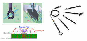
Figure 3: The larger the size of the E-field and H-field probes, the greater their sensitivity, at the cost of precision. It helps to zero in on the EMI source by reducing the size of the probe.
It’s hard to isolate the EUT completely, so the key is to get a baseline measurement against the limit line set up on the spectrum analyzer, accounting for signals that are present. When setting compliance limits for the spectrum analyzer, this can be done manually or using Elektra PC EMI test software on the FPC1000 analyzer. This will help identify problem areas to be investigated further. A respectable spectrum analyzer is likely the closest to a full-compliance EMI receiver a designer will get at low cost (Figure 2). A full EMI receiver is top-tier equipment with lots of expensive filters to help with dynamic range.
The spectrum analyzer itself will need at least a quasi-peak (QP) detector with a directional antenna as part of the minimum viable feature sets to approximate a full EMI-compliant receiver. The goal is to not over-design the device. Without enough accuracy in the power measurement with the QP, designers run the risk of adding additional shielding or over-designing the device, which adds weight, time, power consumption and direct costs. The trick is be just good enough to pass the test for full compliance, without going overboard.
The analyzer should have a frequency range from 5 kHz to 1 GHz (upgradable to 3 GHz if need be), and a built-in vector network analyzer (VNA). The VNA is a useful feature as this can be used to match the antenna impedance to the RF module if there isn’t an RF antenna built in.
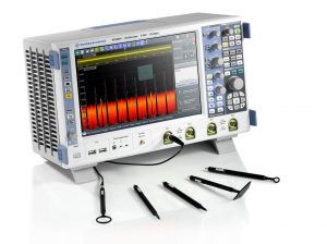
RTO2000 oscilloscopes used for EMI Debug.
Some spectrum analyzers go further and actually integrate a signal generator to form a “three-in-one” instrument. The signal generator can be used to generate an additional signal in the presence of the intended transmitter signal. This “interferer” tests to make sure there is sufficient blocking at the receiver to allow the intended signal to get through.
To start pre-compliance testing, do a limit-line test, or max hold sweep, with a max hold detector, as that’s a fast and easy test. Then, use the QP detector to do spot checks on any potential problem areas. Use electric field (E-field) and magnetic field (H-field) near-field probes (Figure 3). The magnetic field probe has a loop through, which the magnetic field passes perpendicularly, inducing a detectable voltage.
When using the probes, it’s important to keep in mind that the output of the probe very much depends upon the orientation of the probe relative to the emitters. Also, there is a trade-off to be made: the larger the probe, the greater the sensitivity, but the precision decreases. So, as the source of EMI gets more clearly defined, reduce the size of the probe in order to zero in on the source and verify that the readings are below the maximum allowable power levels.
This requires having a solid knowledge of the design to know where these might be. Many EMIs can be anticipated by factoring in the clock frequencies, the power supply’s switching frequency, and the expected harmonics.
Knowing the layout is critical as it helps to know when a clock line might be too close to an RF module. This becomes something to watch for as it might be what’s coupling in and causing another spur that’s in a different part of the spectrum.
However, no matter how good a designer’s knowledge of the physical layout and the circuit’s design parameters, nothing beats running the system software and time-correlating the EMI to the running code.
Time-correlated EMI testing and debug with an oscilloscope
While a spectrum analyzer is an affordable option to a full EMI compliance receiver, the venerable oscilloscope has a critical role to play here, especially during debug. Look for an oscilloscope with these key characteristics: 50-Ω coupling impedance to ensure sufficient bandwidth; a sample rate >2x the maximum frequency (i.e., start with 2.5 Gsamples/s for 0 to 1 GHz); low noise; good vertical sensitivity capable of being set to 1 to 5 mV per division while maintaining full bandwidth.
As the probe will be moving around the board or system, it’s important that the scope’s response time be fast so there’s no delay when trying to correlate EMI back to the time domain. Some scope’s hardware accelerate the FFT to ensure the time and frequency domain are seen in real time. As the source of the EMI becomes clearer, the time-domain view should allow the EMI source to be correlated to changes such as bus level switching.
Other features to look for on a scope include a color table and screen persistence to easily detect and distinguish continuous wave signals and burst signals; signal zoom and fast Fourier transform (FFT) gating to easily isolate spurious spectral components in the time domain. These are features typical of the RTE1000 or RTO2000 oscilloscopes (Figure 4).
It’s possible to use lower cost scopes, but that sacrifices some frequency-domain capability which is important during EMI debug.

Rich Markley is Product Manager for Rohde & Schwarz’s Value Instruments.
Conclusion
Adding RF to an IoT device is tricky, even if RF modules are used. The module may be EMI compliant by itself, but when added to a real-world system, with power supplies, clocks and parasitics, all in smaller form factors at lower power rails, the whole system needs to be checked. While compliance testing is expensive, it can be limited to one formal test by performing pre-compliance testing using basic equipment and some classic best practices.