Extending coin cell battery life in wearable applications
By Majid Dadafshar principal engineer field application engineering, ON-Semiconductor
Electronics Power Supply / Management Semiconductors Supply ChainMost low-power wireless interfaces like Bluetooth, ZigBee and Wi-Fi can be found in many Internet of Things, wearable, medical, health and fitness applications. These mobile applications require a small size coin-cell battery that can function for many months or even years without attention or replacement.
As Internet using standardized communication protocols is getting connected to more of our embedded hardware devices, the next step in “connected world” is to connect our multiple devices at our homes or our environment with the capability to connect and communicate to the existing Internet infrastructure. Some of these devices like wearable health monitoring devices, medical patches, moisture sensors inside walls to name a few, will be operated using a small coin cell battery. Long life expectancy of these batteries is one of the critical factors for successful merging of both the Internet and devices. Designing wearable to meet consumers expectation of higher functionality, high throughput connectivity, small size and longer battery life is a challenging task and this article will try to provide an overview and basic understanding of power blocks, effects of beacons, beacon interval, maximum throughput, transmit packet size in estimating the life for a coin cell battery.
INTRODUCTION:
Having a network of physical devices that can interact with each other and be able to share information in order to take a proper action, like notifying the user when the coffee is ready, dryer is done or when there is a water leak inside of our walls can be very useful information to have. Cost of maintenance or battery replacement can be an obstacle in adoption of these wearable or Internet of Things devices and is crucial to have a good understanding of different sections used in these circuits and a mean to properly estimate the battery life or a time in between the batteries replacement.
The Internet of Things can also be very beneficial in health care applications with using sensors to measure and monitor various medical parameters in the human body. This will allow the care providers to monitor a patient’s health (heart rate, pulse, blood pressure, body temperature, and blood glucose) when they are physically outside a hospital. The wearable devices like smart watches, wristbands, monitoring patches that are pasted on the skin or even smart textiles can provide real time information to the health care provider thru a secured cloud computing data base platform. In the case of monitoring patches, they are supposed to be worn by the patient for a few days or longer and with many smart devices being battery powered, this mandates a need to operate at low power and also to have an efficient power solution.
Building Block of a wearable System:
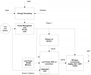
FIGURE 1. Typical block diagram for wearable device.
Five sections form the basic building blocks of a wearable device, including a coin cell battery, power section, sensors, low power ASIC or a processors and RF section. Each of these nodes has to have their own characteristics in order to form an efficient smart wearable device.
Environmental sensors, collecting physical environment parameters like temperature, humidity, pressure, water and air pollution or medical sensors collecting various medical parameters in the human body or any other sensors (medical, accelerometer, gas, moisture), all collect real time data from their surroundings and send to the low power ASIC for processing.

FIGURE 2. – Typical wearable sensor device.
The collected sensor data can be stored and analyzed, by the low power ASIC or a processor in order to create a useful intelligence out of the collected data and in some Miniature Implantable Medical Devices (MIMDs) it might require a development of new category of Application Specific Integrated Circuits (ASICs). New low power ASICs can be designed to perform very specific functions, which reduces both the size of the circuits and the power required to run them. Since a low power ASICs use just the energy needed for a specific task, no energy is wasted on unnecessary functions and can run on smaller batteries to further enable device size reduction or extend the battery life.
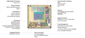
FIGURE 3. Typical example of an ASIC.
The collected sensor data can be stored and analyzed, by the low power ASIC or a processor in order to create a useful intelligence out of the collected data and in some Miniature Implantable Medical Devices (MIMDs) it might require a development of new category of Application Specific Integrated Circuits (ASICs). New low power ASICs can be designed to perform very specific functions, which reduces both the size of the circuits and the power required to run them. Since a low power ASICs use just the energy needed for a specific task, no energy is wasted on unnecessary functions and can run on smaller batteries to further enable device size reduction or extend the battery life.
Key points for processor chips are using low power technologies to reduce internal operating voltage, reducing the onboard oscillator frequency to a low speed during standby and optimize the circuits to reduce power consumption. For any logic blocks both at active or standby mode, there are some solutions in the semiconductor industry to help reduce these losses.
Clock gating is one technique that can be used to reduce the active power dissipation in a system by turning on the clocks (not the power) to specific logic blocks only
when there are tasks pending. When there are no pending tasks, the clocks to a specific logic blocks can be turned off, reducing the active power for that block only.
In many medical applications the low power ASIC or a processors are responsible for securing the data by performing encryption and decryption of the received data before transmitting the sensed data wirelessly (PAN, WAN or LAN) to a gateway and finally to a remote cloud-based end-to-end connectivity platform.
The combined sensor, processor, transmission path and gateway, operate in conjunction with a user controlled application (home automation apps, security, retail, tracking etc.) which are essential for proper utilization of all the data collected. When selecting a wireless technology for your final application, you have to consider factors like, expected battery life, maximum throughput (Mbps), power consumption, maximum distance range and whether you need to connect your device to the internet thru Wi-Fi.
Now, let’s look at an example of a wearable design using a Wi-Fi and try to find out the effect of size of data collected, speed of transmission, security, packet size transmitted, pulsed loads, etc. on power consumption and expected battery life.
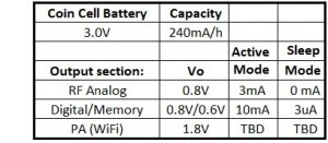
TABLE 1. Preliminary design requirements.
The above table doesn’t contain enough info to provide a complete design but it allows us to come up with a preliminary power block diagram.
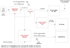
FIGURE 4. – Power block diagram.
Another solution besides clock gating described earlier, is to turn off power to those blocks that are not being used. Power Amplifier (PA) section for Wi-Fi or any other wireless protocol is the main power consumption section and can be switched on/off using a load switch.
Now, we need to calculate the current draw from the PA from its RF power in dBm. For example the RF power for Wi-Fi operating at 2.4GHz could be around 17dBm (50mW), 16dBm (40mW) at 5GHz operation and 20dBm (100mW) as the maximum allowable RF power emission set by regulatory limits.
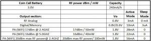
TABLE 2. Design requirement including PA power.
Each transmission would result in the other side to send back an ACK, so there will be transmit and receive for each transmission and the current will fluctuate from TX to RX. The TX current (30+mA) is higher than RX current (5mA) with active TX/RX duration in 2msec range with the rest of time being at either SLEEP or receive of beacon mode. Many power amplifiers (PA) or RF transmitters in a wearable device spend most of their time in sleep mode and only send the measured and processed data on a very low duty cycle basis. They also consume a considerable amount of power, so before attempting to estimate the battery life, we need to be able calculate the average power by finding out more timing details.
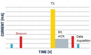
FIGURE 5. – Transmit profile.
The duration of actual transmission depends on many factors like the byte size, number of packets, beacon interval, encoding overhead of data and overall number of bits to be transmitted.
For example with 5 packets of 200 bytes and 40% encoding overhead, it translates into 11200 total bits to be transmitted. With the data throughput of around 2.75Mbps for Wi-Fi transmission, it will take 407us (TX on Fig 5.) to transmit 11200 bits of data.
In WLAN 802.11 wireless protocol, there are data frames to carry information and management frames to support data transfer. The beacon frames are type of management frames that can be set through the access point configuration which enables any stations to establish and maintain communications. Beacon signals and used as a discovery mechanism with around -40dBm to +4dBm power range for broadcasting its signal. The beacon frames lead to more overhead or bits and will cause more power dissipation. Each beacon frame carries information like beacon interval 100-2000ms which represents the time between each beacon transmissions and are usually about 50 bytes long.
When a station is entering into a power save mode, it needs to know the beacon interval so it could wake up at a right time to receive the beacon and update its local clock for proper timing synchronization among all stations that are communicating with a given access point. The shorter the beacon interval, the more stable the signal but it also can significant impact to the battery life.
Each beacon also carries information that indicates the data rates that the WLAN supports, like 1, 2, and 5.5Mbps, etc. By increasing the beacon interval, we can reduce the number of beacons, overhead and make the association and roaming process less responsive. We can also decrease the beacon interval, causing an increase in the rate of beacons and overhead which will cause additional devices using power save mode to consume more power since they’ll need to awaken more often, effectively reducing power saving mode benefits.
We also need our own tool so we could input all different parameters for different applications and look at entire design parameters in order to drive our power consumption calculation and estimating battery life.
TABLE 3. Effects of changing design parameters on battery life.
The shorter the beacon intervals, the shorter the battery life, but the faster the device can be discovered. Broadcasting power directly impacts signal range and more power equates to a longer the range. Increasing the power can also make the signal more stable, but keep in mind it can have a negative effect on battery life.
Since the active power is a function of both supply voltage and frequency (Freq * V^2), we can control the active power by dynamically controlling the supply voltage or by modulating the clock frequency of the processor as a function of the intensity of the computing task. When less performance is required or during sleep mode, the system can either lower the frequency or lower the supply voltage to the system.
The new trend in power management to improve the overall power dissipation is using a Super Low IQ (SLIQ) DC-DC and LDO with “Mode Select” capability.
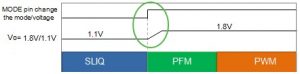
FIGURE 7. SLIQ operation mode for DC-DC.
By lowering the output voltage of the DC-DC for SLIQ or sleep mode, the voltage across the LDO can also be reduced, causing lower power dissipation across the LDO devices.
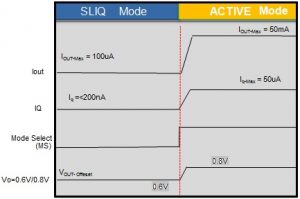
FIGURE 8. SLIQ operation mode for LDO.
The benefits in this design approach using SLIQ DC-DC or SLIQ LDO is the ability in changing or lowering the IQ when transitioning from active mode to SLIQ mode. They can also change their output voltages with a pre-selectable manufactured settable offset voltages, so the output voltage can be changed from a higher voltage (0.8V) during active mode to a lower output voltage (0.6V) when transitioning to SLIQ mode, for example during memory retention.
Conclusion:
In order for wearable device to extend battery life, a proper design need to consider low power ASIC that can perform heavy computational with minimum of power usage. The wireless connectivity protocols like Bluetooth Smart and ZigBee with power amplifier (PA) in the radio side, power-ICs and sensors with low leakage currents, all need to be specifically designed for ultra-low-power applications. For a coin cell battery to last several months or even years, data rate, beacon interval and transmit time, all have to be considered in order to lower the average current draw to a few tens of milliamps (mA) when operating in active mode and few (nA) when in sleep mode.
Using load switch to actively disconnect Power amplifier and digital section from the supply rails can also have a significant effect in lowering the power consumption of different sections when they are not used. Using a Super Low IQ (SLIQ) DC-DC and passing their output through an SLIQ LDO with both low voltage drop and “MODE” select pin can also lower the power consumption and extend battery life.
——————————————————————————————————-

Majid Dadafshar
Majid Dadafshar is working for ON-Semiconductor as Principal Field Application Engineer. He has over 33 years of design engineering experience in power electronics, both in commercial and military applications. He has been employed by Fairchild Semiconductor, Maxim integrated, ITT Power systems, ITT courier, ITT Aerospace/Defense, Sony Electronics, Eastman Kodak, and Pulse Engineering. He holds 4 Patents and has published a number of technical papers in power supply designs, magnetic, EMI, loop stability, MEMS, RFPA and conducted numerous domestic and international electronic technical meetings in different symposiums.