10nm Process rollout marching right along
By Andy Wei, senior technology fellow, TechInsights
Electronics Embedded Systems Engineering Supply Chain 10nm class embeddedThe first set of Samsung Galaxy S8 teardowns provided access to the first SoCs produced on “10 nm” class technology. The first company to produce the 10 nm was Qualcomm with the Snapdragon 835, which was built on Samsung LSI Foundry’s 10LPE technology. In parallel, Samsung’s Exynos 8895 was released followed by the Apple A10X, which was built on TSMC’s 10FF process. 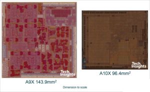
Qualcomm Snapdragon 835 vs. Snapdragon 820/821
The Qualcomm Snapdragon 835 has a die size of 72.3 mm2, which is a 36% die size shrink when compared to the die size of the Snapdragon 820 at 113.7 mm2. It appears to be a shrink of the Snapdragon 820/821 family. While it has upgrades to similar IP blocks as in the 820/821family, no major new IP blocks were added.
The biggest change identified by TechInsights is in the CPUs. The Snapdragon 820 family used a very large area, 2+2 big-little implementation, which seemed out of place for a mobile applications processor. We suspect the Kryo was a re-use of cores designed for Qualcomm’s ARM-based server products. The Snapdragon 835, however, uses a more ARM-like 4+4 big-little implementation in the Kryo 280, as they appear to be a derivative of the ARM Coretex-A73/A53 implementation we saw in the HiSilicon Kirin 960.
This major change in CPUs skews the overall die size reduction giving the appearance of a more significant scale factor. However, looking at functional blocks with more minor changes, such as the Adreno 530 to Adreno 540 GPU MP unit, the reduction is a similar 36% area scale. Without further, detailed analysis, it is not clear whether this indicates the true scale factor or the result of a concurrent increase in complexity to take advantage of the area scale.
In evaluating implementations of Samsung’s 10LPE technology, TechInsights is currently looking closely at the standard cell level and routing. This allowed our analysts to gauge actual routed gate density gains and cost per gate scaling improvement.
Apple A10X
The A10X die size comes in at 96.4 mm2 as compared to the previous generation, A9X at 143.9 mm2, which was built on TSMC’s 16 FF-Turbo technology. This is an impressive full node scale, when accounting for the extra CPU cores built into the A10X and extra IP blocks of the A10 vs. A9 family. TechInsights estimates a 45% die level scale (0.55x the area of running on the previous technology), based on our detailed floorplan analyses of the Apple A-series.
The Apple A10X examined was extracted out of the new iPad Pro2, which was introduced in June 2017. It’s interesting to note that the original rumored release date for this iPad was in March. This meant it would have had to align with TSMC’s “Night Hawk” program’s stated goal to accelerate 10FF R&D in order to beat Samsung 10LPE’s known launch date of April 2017. The 1Q delay, along with well-known design losses of MediaTek’s Helio X30, also designed on TSMC 10FF, indicates a slower than anticipated ramp for this technology. These delays, along with TSMC’s statements that 10FF will be a short-lived technology that will be supplanted by 7FF in 2018, indicates some non-ideal performance/power, area, and cost factors for 10FF. 
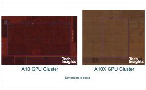
At an IP-block level, TechInsights compared the GPU between A10 and A10X, which appear to be the same Apple customized Imagination PowerVR cores. This showed ~49% area scale (0.51x the area of running on the previous technology). This would indeed point to an impressive full node scale, and will be verified as we look closely at the standard cell level and routing of Apple’s implementation of TSMC 10FF.
Node Confusion
There is currently confusion around what a technology node name actually means, as the node names have been decoupled from physical pitch or even scale factor. Unfortunately, this confusion will only continue moving forward. Samsung 10LPE scale factor vs. Samsung 14LPP, for example, was only 36% at the IP block level, and node names have been announced down to “4LPP.” Intel, on the other hand, has announced their 10 nm to be “hyperscaled” compared to their 14 nm, which according to their metric would lead to ~63% IP block level area scaling. Adding to the confusion, 10 nm will likely be a long-lived node for both Samsung and Intel, and a short-lived node for TSMC, with multiple “7 nm” technologies around the corner, and a slew of other node names and node variants in-between. The marketing battle is fierce for the hearts and minds of companies locked in battles to dominate high margin mobile, data center infrastructure, and looking to win in the race to 5G, automotive automation, and pervasive artificial intelligence.
This is an exciting time. Rather than an abrupt end to Moore’s Law scaling as many industry analysts had predicted, we are finding ourselves in the midst of very high innovation to overcome physical scaling limits and maintain traditional cost and performance scaling. TechInsights will continue to analyze entries into the “10 nm” class technology and provide insight on how they fare compared to the players at 14/16 nm, and what the future holds for sub-10 nm.
As our in-depth analyses at the functional block floorplan level, standard cell library, utilization, process analysis, and transistor characterization conclude, we will offer insights to what’s inside technology through our SoC Design Architecture program.