Astera Labs unveils Burnaby B.C. location
EP&T Magazine
Automation / Robotics Electronics Semiconductors Engineering IoT Supply Chain AI connectivity semiconductorsNew design center and state-of-the-art lab to lead in purpose-built connectivity solutions for AI & ML infrastructure
Astera Labs, a Santa Clara CA-based provider of purpose-built connectivity solutions for intelligent and accelerated systems, has celebrated the grand opening of Astera Labs Vancouver – a new office and state-of-the-art lab to support the company’s development of cutting-edge interconnect technologies for Artificial Intelligence and Machine Learning architectures. The new location will tap into the region’s rich technology talent base to drive product development, customer support and marketing.
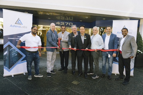
Astera Labs executives host Burnaby Mayor Mike Hurley and Burnaby Board of Trade CEO Paul Holden for its new design center and state-of-the-art lab ribbon cutting ceremony. Pictured from left to right: Kush Saxena, Mayor Mike Hurley, Sanjay Gajendra, Paul Holden, James Wang, Mike Hillman, Dave Nelson, Sanjay Charagulla. (Source: Business Wire)
“We are in a tremendous growth phase in every aspect of our business and the new Astera Labs Vancouver location will be instrumental in driving our continued expansion as a company and as the industry leader in advanced data and memory connectivity,” said Sanjay Gajendra, chief business officer, Astera Labs. “We will accelerate our vision to enable the true potential of AI and Machine Learning in the cloud with our purpose-built intelligent connectivity solutions.”
The Vancouver area is a suitable location for Astera Labs’ expansion given its reputation as a leading North American technology hub and strong university ecosystem. Astera Labs is actively hiring across multiple engineering and marketing disciplines to support end-to-end product and application development and overall go-to-market operations.
Continue to expand our presence in Canada
“We are thrilled to welcome Astera Labs and support its continued growth as a rising-star in the global semiconductor industry,” said Mike Hurley, Mayor of Burnaby. “The company’s investment in Burnaby will bring significant job opportunities to our region and underscores the immense value that our talented workforce can offer to technology leaders like Astera Labs.”
“We greatly appreciate the City of Burnaby for celebrating this momentous occasion with us and look forward to its ongoing support as we continue to expand our presence in Canada,” said Dave Nelson, senior director product applications and site leader, Astera Labs Vancouver.
The new Astera Labs Vancouver office increases the company’s operations in Canada, which already includes the new Research and Development Design Center in Toronto, and adds to its global footprint with headquarters in Santa Clara, California and offices around the globe. To view open positions and apply, visit www.AsteraLabs.com/Careers/.