Layered materials grant sight to electronic chips
EP&T Magazine
Electronics Semiconductors Engineering artificial chips Flagship graphene materials network Neural semiconductorsChip based on layered materials classifies images a thousand times faster than conventional machine-vision systems
Researchers at Graphene Flagship partner, the Vienna University of Technology in Austria, has reported an image sensor with an integrated artificial neural network (ANN) capable of learning and classifying images within nanoseconds. The chip is a thousand times faster and uses much less power than conventional vision technologies.
The image sensor can simultaneously capture and process images, making object recognition many orders of magnitude faster. The device does not consume any electrical power when it is operating, since the photons themselves provide the energy for the electric current. The sensor is complemented by an ANN, a man-made system inspired by our brain. In an ANN, components dubbed “neurons” are fed data and cooperate to tackle a problem. In this case, recognizing an image.
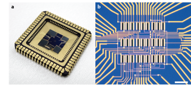
Devised sensors containing nine pixels

Source: Graphene Flagship
The researchers in Vienna, supported by the European research project, the Graphene Flagship, devised sensors containing nine pixels – the ‘neurons’ – placed in a 3×3 array. Every pixel in turn, consists of three photodiodes, which are semiconductor devices that convert light into electrical current, that provide three outputs. Each photodiode links its pixel to the other 8 pixels. The current from each photodiode is determined by the intensity of incoming light and the voltage across it. Each neuron sums the individual currents coming from the other 8 neurons, and the combined values are then fed into a computer.
The device can classify images after a series of training processes, but it can also recognise a characteristic component or structure of an image from input data, without extra information. The speed sets this device apart from conventional machine vision. Conventional technology is usually capable of processing up to 100 frames per second, with some faster systems capable of working up to 1,000 frames per second. In comparison, this system works with an equivalent of 20 million frames per second. It has been suggested that the device will be scaled up with today’s technology and find applications in different fields, such as fluid dynamics, high-energy physics, combustion processes or mechanical breakdown.
Audio or olfactory neuromorphic sensors
“Scaling the devices up, this neuromorphic approach can play out its strengths in the realm of image recognition and processing,” explains Lukas Mennel, first author of the study. “We are also considering other ideas, like improving the light absorption or extending the spectral range into the infrared. In principle, the capabilities of this device are not only limited to visual data. Any kind of data could be (pre)processed with an artificial neural network in the sensor itself. For example, audio or olfactory neuromorphic sensors could be developed for rapid on-chip processing.”
Source: Graphene Flagship
“This impressive work shows a completely new application of layered material-based cameras, taking advantage of its unique properties like its in-situ tunability.” explained Frank Koppens, Graphene Flagship work package Lleader for Photonics and Optoelectronics. “Neural network image sensors will impact society in many different ways, and with layered materials the high-speed requirements have now been met.”
Andrea C. Ferrari, Science and Technology Officer of the Graphene Flagship and Chair of its Management Panel, added: “This work is another major milestone for the Graphene Flagship. The Flagship is clearly world-leading when it comes to the integration into chips of layered materials. These advanced building blocks will underpin the development of new state-of-the-art technologies.”
Backgrounder
The Graphene Flagship is a research, innovation and collaboration project funded by the European Commission. The Graphene Flagship aims to secure a major role for Europe in the ongoing technological revolution, helping to bring graphene innovation out of the lab and into commercial applications. The organization gathers nearly 170 academic and industrial partners from 21 countries, all exploring different aspects of graphene and related materials. Bringing diverse competencies together, the Graphene Flagship facilitates cooperation between its partners, accelerating the timeline for industry acceptance of graphene technologies.
For more information on this Graphene Flagship research, click here.