Seven DFM Issues Potentially Lurking in Your Design
By EMA Design Automation Inc.
Electronics Engineering Software Production / Materials Engineering Supply Chain DFM issues DFM issues pcb pcb pcb production pcb production printed circuit boardsAvoid Troublesome Design for Manufacture (DFM) Errors in the Production Process of Your Printed Circuit Board (PCB)
Does this situation sound familiar? You complete your design and send it off to the fabrication house only to have your product put on hold for numerous DFM (design for manufacture) errors. Being in this situation can not only be frustrating, but costly as well.
Considering manufacturing issues early within your project timeline helps to lower cost, reduce development time, and ensure a smooth transition into production. Not doing so, all but guarantees the opposite.
From conversations with customers and our years of industry involvement, we have complied a list of the top DFM issues which prevent printed circuit board (pcb) manufacturability. While some of what is listed below can be considered design best practices, others are put in place by the fabrication/manufacturing house themselves. By fixing these issues in the design phase of your project, you will be able to correct any potential DFM issues before it gets to the shop.
So, before you send your designs off to manufacture, look out for the DFM issues we have listed below, as they may be lurking in your design.
1. Acid Traps 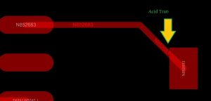
When we are discussing Acid Traps, we are describing acute or odd angles of copper features on the printed circuit board which cause acid to pool during the pcb creation process. This issue occurs before the wash process, where acid traps allow for residual acid to get caught in these areas and not get cleared away. As a result, the wanted copper features the Gerber file included on the board begin to erode, creating “opens” or lost copper connections.
Avoiding acid traps are especially important with the 4 or 5 mil traces on today’s designs. Since they are so thin, they can easily become opens (openings created within wanted copper due to trapped acid). Some software has built in checks for these, however, if your software does not, you will have to manually evaluate the board for anything that could cause this.
How to prevent Acid Traps: Avoid placing the trace coming into a pad at an acute or odd angle. Keep angles 45 or 90 degrees adjacent to the pad.
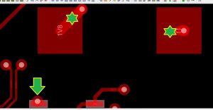
2. Slivers and Islands 
Slivers and islands are free floating copper on many plane layers that can create some serious problem in the acid tank. Several issues can occur because of this. The small specks of copper have been known to float off the pcb panel and find their way to other etch on the panel creating a short.
Or, if they are large enough to not be able to float off it becomes your antenna, which can cause noise and other interference within the board (because its copper with nothing grounding it—it becomes a signal gatherer). Some software can search for these within your design, however, if your software does not have this capability, you will have to manually find and remove them from the board design.
Note: There is no surefire way to avoid silvers and islands. However, they are something you or your software must check for.
3. Solder Bridges Forming Between Pins
With etch traces being so fine-lined and pin-pitch so tight, it is essential to include soldermasks within a pcb design. Excluding soldermasks can result in a large blob of solder (especially between pins) during assembly–resulting in a short. In addition, it can also cause reduced corrosion protection on other copper on the outside layers.
To help prevent these issues, be sure to check the alignment, soldermask to soldermask (webbing) spacing from pad to etch lines and to shapes. Also, be sure there is no soldermask covering pins—your board house can inform you on the minimum webbing space and alignment they will allow.
4. Heat Sinks
Heatsinks absorb and dissipate heat from an electronic component through contact with a metal base or thermal interface material. If the pastemask openings are too large in the heat sink, once the solderpaste melts it could cause components to float off the pads. To prevent this, reduce how much paste is put down on a heat pad—instead of one large paste mask opening, try breaking it up into several, smaller paste mask openings. This will help to ensure components will not float and crash into other parts during the oven process, which can shorts.
Pastemask openings are an essential part of DFM checks. Before sending off to manufacture, ask yourself: Do all the component leads on the pcb have the proper pastemask opening (and size) for the stencil?
Note: Your manufacturing engineer should be able to provide you with what the proper size of your pastemask opening should be.
5. Cold Solder Joints or No Solder Connection
Checks for vias within pads are essential—if the via is not properly placed, it could allow solder paste to flow down into the via. This will result in a cold solder joint or no real solder connection. You need to find out: What percentage of the via is allowed in the pad before plugging the via is a requirement. Note: It’s the hole in the via that creates the problem, not the pad in the via.
Most software should be capable of checking for these issues, however if yours does not, you will have to manually check your design to be sure it is in compliance with your assembly house criteria.
6. Test Points are Not Included
It is important to include a way to test your final product once they are off the assembly lines—by including test points in your initial design, you are providing a way to audit the success or failure of a board once it has been completed. DFM checks must include test point to component clearances, pad size, under components, and a way to lock down these locations once a fixture is built.
Test point data is then used to create a fixture known as the Bed of Nails Tester. A bed of nails tester is a software system that locks your test point locations down within the design. They provide you with the ability to allow for a design change to be reworked into this test fixture, ultimately saving money.
If you wait to include test points until after your prototype has been completed, you could alter the electronics on the board (which could create crosstalk, noise, and a whole host of other issues) and therefore not really test the board’s true functionality. You will essentially be changing the design and how the board operates. By incorporating the test points into your board during the design phase, it provides you with the ability to lock down what’s there and only modify any changes.
Items to keep in mind when adding test points to your design: Are they accessible? Does the DM checker make sure your points are not hidden? How is the pin spacing (be sure they are not too close together)?
Note: When you put the test points on the board, they become part of DFM checking.
7. Copper to Board Edge
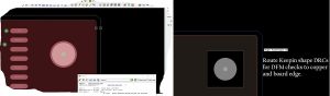
Part of the pcb creation process includes the motorized transport of boards into acid and wash baths. The copper to board edge is the space on the grip the side of the pcb panels used to transport the boards throughout the manufacturing process. If the proper spacing between the copper to board edge is not set appropriately true manufacturing issues can be created. If the copper is too close to the edge of the board, shorts can be created when the electrical current is applied to the panel during the etching processes.
Note: The equipment being used to manufacture the boards will be what controls the spacing needed to grip the panel—your board fabricator should be able to provide you with design specifications.
The consequences of manufacturing failure are not only frustrating, but costly. Planning for the future by designing for manufacture is just one of the many ways to avoid running into issues during manufacturing. The good news is, many of the issues listed above can be automatically identified using software (OrCAD 17.2 comes armed with OrCAD DesignTrueTM In-Design DFM Technology). However, if your software does not have DFM checking capabilities, you will have to manually identify and resolve them yourself.
The last thing any engineer wants is to receive ‘the call’ from their manufacturer stating their board has failed their DFM checks, so it is important to look for the above issues in your final checks—whether that’s through automated or manual checks.
For more information on design for manufacturing, other pcb design-related topics, or you want to learn more about OrCAD products visit www.ema-eda.com.