Conductive inks: conformal 3D-shaped coatings are a game-changing success?
By Dr Khasha Ghaffarzadeh, Research Director, IDTechEx
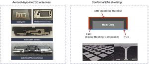
Electronics Production / Materials Supply Chain 3D-shaped 3D-shaped Conductive inks conductive inks EMI shielding EMI shieldingA major frontier in the conductive ink business is conformal coating on 3D-shaped objects. For the purposes of this article, this will be divided into two categories as shown below: aerosol-deposited 3D-shaped antennas and conformal on-chip EMI shielding. The IDTechEx Research report Conductive Ink Markets 2018-2028: Forecasts, Technologies, Players shows how one is already a growing success whilst the other is amongst the hottest trends in the conductive ink business.
Aerosol deposition: Gateways to success are open
First lets briefly consider aerosol deposited antennas. Aerosol deposition is digitally controlled and benefits from fewer process steps and a lower machine footprint compared to the main competition LSD (laser direct structure) which also includes a plating step. The aerosol-compatible conductive inks- composed mainly of nano sized or sub micron particles- need to have tight control on particle size distribution so that the jetted lines remain uniform. An ongoing area of development is improving the adhesion and achieving higher conductivity levels at lower temperatures and shorter curing times. After all, performance wise, the competition is plated metallization tracks.
The good news is that this application has been making steady progress. Today, multiple industrial scale aerosol machines have been installed worldwide, opening the gateways to ink sales.
Source: IDTechEx Research report Conductive Ink Markets 2018-2028: Forecasts, Technologies, Players.
Sprayed on-chip conformal EMI shielding: the hottest market trend?
The second category is conformal on-chip EMI shielding. This is amongst the hottest trends in the conductive ink space. EMI (electromagnetic interference) is a growing issue in electronic devices where multiple ICs are packaged in a small space. Of course, EMI shielding could be achieved using bulky and inexpensive metallic cages. This approach however would add to total thickness, which would be unacceptable in consumer electronic devices where the industry exerts concentrated effort to continually thin devices. This is where conformal coating comes in: a thin conductive ink is applied conformally onto the chip package (onto the epoxy moulding compounds). It may be more expensive, but it is thin.
It is already used in, for example, iPhone 7 where several ICs have such coatings. These coatings are however based on sputtered silver. Sputtering is a known and available technology that gives highly conductive, and thus thin for a given EMI shielding performance level, lines. Ink spraying, however, is being positioned as a viable and highly attractive to sputtering. This is because unlike sputtering, spraying is a non-vacuum process that can be easily scaled to large areas. Furthermore, it is a low-Cap deposition technique that gives highly conformal coverage with excellent side-wall coverage. Here also the inks can be appropriately formulated to improve adhesion. These are all attributes that sputtered versions lack.
Nano inks would offer high conductivity
The coated lines, however, may not be as conductive as well sputtered solid-like thin film coating. This gives interesting dynamics in terms of the preferred choice of ink technology. Nano inks would offer high conductivity and thus higher thinness but come at a cost. Micron-sized spherical-type particles are cheap but not as conductive. Planar flake type particles can give high in-plane conductivity but achieving good side coverage requires optimization. Hybrid versions might hit the sweet spot but that must be proven in evaluations. This dynamic is playing out today.
The spraying technology is already qualified for use on a memory chip. The main ink suppliers present in the final qualification round were both Korean and reliability turned out to be determining factor. The question now is will this technology be adopted by other brands and will it move beyond memory? Despite the sunk cost of CapEx in sputtering machines being a short-term barrier against the adoption of alternative approaches, the engagement is now very strong particularly in China and the market is now eagerly awaiting a proper reference. This is a space to watch with a large addressable market in which spraying inks offers a compelling value proposition. Indeed, success in this market could change the fortunes of various conductive ink technologies.