3D electronics enables greater integration with objects
By Dr Matt Dyson, senior technology analyst, IDTechEx, Cambridge, UK
Automation / Robotics Electronics Production / Materials Engineering Printable Electronics 3D pcbs printing3D electronics is an emerging manufacturing approach that enables electronics to be integrated within or onto the surface of objects. While it has long been used for adding antennas and simple conductive interconnects to the surface of 3D injection-molded plastic objects, more complex circuits are increasingly being added onto surfaces made from a variety of materials by utilizing new techniques.
Furthermore, 3D additive electronics enables complete circuits to be integrated within an object, offering multiple benefits that include simplified manufacturing and novel form factors. With 3D electronics, adding electronic functionality no longer requires incorporating a rigid, planar PCB into an object then wiring up the relevant switches, sensors, power sources, and other external components.
There are three main approaches to 3D electronics, each discussed in detail in a recent report released by IDTechEx.
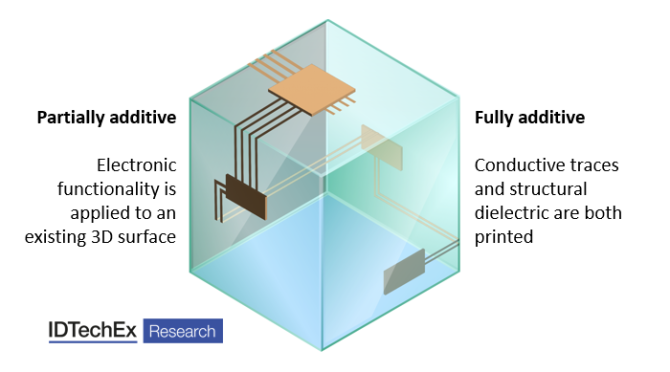
Fig 1: Contrasting approaches to 3D electronics. Source: IDTechEx
Applying electronics to a 3D surface
The most established approach to adding electrical functionality onto the surface of 3D objects is laser direct structuring (LDS), in which an additive in the injection-molded plastic is selectively activated by a laser. This forms a pattern that is subsequently metalized using electroless plating. LDS saw tremendous growth around a decade ago and is used to manufacture 100s of millions of devices each year, around 75% of which are antennas. However, this metallization method can only be applied to injection molded components with an additive, and only enables a single metal layer to be deposited thus limiting circuit complexity.
Given these limitations, other approaches to applying conductive traces to the surfaces of 3D objects are gaining ground. Extruding conductive paste, a viscous suspension comprising multiple conductive flakes, is already used for a small proportion of antennas and is the approach of choice for systems that deposit entire circuits onto 3D surfaces. Aerosol jetting and laser-induced forward transfer (LIFT) are other emerging digital deposition technologies, both of which have higher resolutions and rapid deposition of a wide range of materials respectively.
In-mold electronics
In-mold electronics (IME), in which electronics are printed/mounted prior to thermoforming into a 3D component, facilitates the transition towards greater integration of electronics, especially where capacitive touch sensing and lighting is required. By enabling multiple integrated functionalities to be incorporated into components with thermoformed 3D surfaces, IME offers multiple advantages relative to conventional mechanical switches, including reduction in weight and material consumption of up to 70% and much simpler assembly.
IME is an extension of well-established in-mold decorating (IMD), in which plastic sheets with a decorative coating are converted to three dimensions via thermoforming and subsequent injection molding. IME differs from IMD through the initial screen printing of conductive thermoformable inks, followed by deposition of electrically conductive adhesives and the mounting of SMDs (surface mount devices, primarily LEDs at present).
The long-term target for IME is to become an established platform technology, much the same as rigid pcbs are today. Once this is achieved getting a component/circuit produced will be a simple matter of sending an electronic design file. Along with greater acceptance of the technology, this will require clear design rules, materials that conform to established standards, and crucially the development of electronic design tools.
Fully printed 3D electronics
Arguably the most innovative approach to additive electronics is fully 3D printed electronics, in which dielectric materials (usually thermoplastics) and conductive materials are sequentially deposited. Combined with placed SMD components, this results in a circuit, potentially with a complex multilayer structure embedded in a 3D plastic object. The core value proposition is that each object and embedded circuit can be manufactured to a different design without the expense of manufacturing masks and molds each time.
Fully 3D printed electronics are thus well suited to applications where a wide range of components need to be manufactured at short notice. The technology is also promising for applications where a customized shape and even functionality is important, for example, medical devices such as hearing aids and prosthetics. The ability of 3D printed electronics to manufacture different components using the same equipment, and the associated decoupling of unit cost and volume, could also enable a transition to on-demand manufacturing.
The challenges for fully 3D printed electronics are that manufacturing is fundamentally a much slower process than making parts via injection molding since each layer needs to be deposited sequentially. While the printing process can be accelerated using multiple nozzles, it is best targeted at applications where the customizability offers a tangible advantage. Ensuring reliability is also a challenge since with embedded electronics post-hoc repairs are impossible – one strategy is using image analysis to check each layer and perform any repairs before the next layer is deposited.
——————————-

Dr Matt Dyson, senior technology analyst, IDTechEx, Cambridge, UK