Waterloo startup NanoCnet rolls out next gen nanomaterial for flexible transparent electrodes
Stephen Law
Electronics Production / Materials Regulations & Standards Engineering IoT Printable Electronics Supply Chain Wearable Technology flexible transparent electrodes nanostructure ink nanotechnology nanotechnologyEP&T Magazine conducted an exclusive Question & Answer session with NanoCnet co-founders Dr. Hadi Hosseinzadeh Khaligh, CEO and Dr. Ehsan Mazbanrad, COO
Company synopsis:
NanoCnet Ltd. is a Waterloo-based startup company established in 2016 with the objective to manufacture silver nanostructure ink and transparent conductive film. 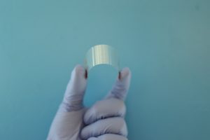
NanoCnet recently introduced a new generation of nanomaterial for flexible transparent electrodes. Highly transparent electrodes, with high electrical conductivity and thermal stability can be fabricated using NanoCnet’s silver based ink called ‘Nanosilvex’. Compared to typical silver nanowire, synthesis process of NanoCnet’s nanomaterial synthesis is faster and happens at room temperature which is ideal for low-cost manufacturing. The unique properties of NanoCnet’s electrodes make them a suitable option for device applications such as touch panels, solar cells, displays, and smart windows.
Q. Describe NanoCnet’s silver nanostructure ink and transparent conductive film for our readers.
A. In general, conductive inks and transparent conductive films are key components widely used in manufacturing many electronic devices including touchscreens, displays, solar cells, sensors and smart windows. Our silver nanostructure ink called ‘Nanosilvex’ is a unique nanomaterial dispersed in an aqueous medium and is compatible with roll-to-roll manufacturing processes. After depositing the ink on a transparent substrate, nanomaterials make a highly conductive network on the surface with lots of empty spaces between them which results in a highly transparent and conductive film. This film can be employed to make high performance, flexible electronics at much lower cost.
Q. Describe the unique properties of these electrodes.
Our ‘Nanosilvex’ ink is produced at room temperature and the whole process takes a few minutes which reduces the manufacturing cost significantly. In addition, their unique structure makes the film highly stable under chemical, mechanical, and thermal stresses. That is essential for durability of the films in devices.

Q. NanoCnet CEO, Dr. Hadi Hosseinzadeh Khaligh, describes how the firm achieved its early success.
A. I received my MASc. and Ph.D. degree in nanotechnology from the University of Waterloo. I spent last 7 years studying transparent conductive films with focus on deficiencies of the current technologies. After I graduated from the University of Waterloo I decided to find a way to address the problems of the existing technologies that I noted during my research and finally found it. I successfully gathered a strong technical team headed by Dr. Ehsan Marzbanrad that could help me to develop a new generation of nanostructures that could solve the cost, flexibility, and durability issues of the current technology. We are working with dedicated aim to be the first in the market with our unique solution.
Q. What are the key advantages of using these products in an electronic design?
A. ‘Nanosilvex’ ink is easy to apply using existing roll-to-roll manufacturing processes. The resulting Nanosilvex film is a low-cost, flexible, and durable option for electronic devices. The high durability means these films can tolerate much higher levels of thermal, electrical, and chemical stresses compared to other competitor’s products on the market.
Q. What are the main (design) applications you anticipate these production materials being used in?
A. Our Nanosilvex ink and transparent conductive film can be integrated in a wide range of applications. The main goal of NanoCnet is to integrate the films into the upcoming printed flexible technologies mainly flexible touch panels, displays, smart device and clothing. 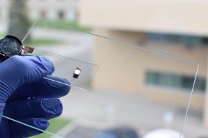
Q. Briefly describe how NanoCnet’s transparent conductive films will lower the cost of manufacturing.
A. Our ink is synthesized at room temperature and ambient pressure and the whole process takes only few minutes. This reduces the manufacturing cost significantly. In addition, we use water-based and eco-friendly chemicals which reduce the raw materials cost as well.
Q. Describe the rise in use and importance anticipated for flexible and printable electronics in the coming years (decade)..
A. Flexible electronics are becoming popular nowadays and even more popular in future. Records shows a market growth rate of 20% per annum. Besides that, the touchscreen market is growing rapidly these years and the market value will be doubled in the next 5 years reaching more than $7B. by year 2022
Q. You are currently operating out of the Accelerator Centre in Waterloo. Describe the importance it has played in assisting NanoCnet through the early start-up phase.
A. The Accelerator has been a great source of help in three main areas of helping us to obtain financial resources, providing access to experts and experienced mentors in all related areas, introducing us to the strong national and international network to help us develop and move toward our mission.
Q. Describe the process of licensing electronic device OEMs to use your technology.
We are currently negotiating with large enterprises to find the best industrial partner to scale up our manufacturing process and potentially license device manufacturing companies to use our products in their devices.
Q. Describe the importance of having strong IP protection.
A. Our technology and development is very unique with unbeatable advantages over existing technologies, therefore, it is very important to make sure the development is fully secured toward all possible claims. We have already filed a provisional registration in US. A complete application with the help of known and experienced Lawyer is in preparation. We will further continue to take all required steps to have full security and claim coverage on international base. Our technology and development being very unique with unbeatable advantages over existing technologies, it is very important to make sure the development is fully secured toward all possible claims. Accordingly the IP protection and license registration is of very high importance for us and we will do all needed to have that full security in place.
Q. Describe the importance of working in concert with smaller tech firms to help perfect your technology, prior to approaching some of the larger end-users of NanoCnet’s products.
A. Working with all Beta manufacturers is highly valued and very important for us. We do have that objective in our mid and long-term agenda. Such cooperation and feedback, as well as the support we get from them help us to recognize any possible bottlenecks and obtain validation from known and credible related industries. Smaller firms’ feedback results in maturing our developments faster by means of adjusting our final products with higher level of quality. This gain will saves us a lot of time and energy in creating a constructive platform to negotiate effectively negotiating with larger companies.