Selecting the right buck-boost converter for wide-VIN rails
By Vijay Choudhary, applications engineer, Texas Instruments
Power Supply / ManagementIntroduction
Buck-boost converters are needed in a variety of applications including USB Power Delivery (USB PD), industrial computer power supplies, LED drivers, and automotive infotainment. Traditionally, cascaded stages or multi-winding, single-stage topologies such as single-ended primary inductor converter (SEPIC) or flyback have been used to generate buck-boost converters.
Two-switch and four-switch buck-boost converters utilize a single inductor and offer advantages such as simplicity, smaller solution size, and/or higher power and greater efficiency. This article presents different buck-boost topologies and explains the advantages and limitations of each. Real hardware design data, simplified equations, and waveforms are used to help the reader compare different topologies. Understanding the topology differences can be the key in selecting the right buck-boost converter for your application.
Need for buck-boost converters
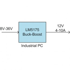
A buck-boost converter is needed when the input voltage range extends both above and below the required output voltage range. Figure 1(a-d) shows some common applications where a buck-boost converter may be needed. The example in Figure 1a shows a buck-boost converter that operates from the 12-V automotive bus varying from 3.5V and 42V to generate fixed output rails. Figure 1b shows an industrial PC power supply working from 8-36V input power and regulating to a 12V output.
The power supplies for power amplifiers (Figure 1c) often need to generate variable or selectable output voltages, depending on the type of power amplifier (PA) they are connected to and the power being delivered. This configuration change can be static or dynamic. System designers often want to use a single power stage to handle multiple load/line voltages and buck-boost is often the only topology that can handle the wide ranges required.
Another common application area is USB PD (Figure 1b) where the input can be a fixed or variable voltage (for example, 12-V battery) and the output voltage (5V, 12, or 20V). The power level is decided after communication is received between source and load.
Buck-boost converters can also replace boost converters where true short circuit protection is desired, or where in-rush current protection is required.
*See Figure 1A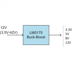 *See Figure 1B
 *See Figure 1C
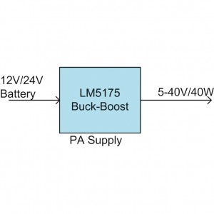
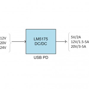
Figure 1. Examples of common applications for buck-boost converters: a) buck-boost converter for infotainment; b) buck-boost need in IPC applications; c) buck-boost for variable PA supply; d) buck-boost for USB PD.
Buck-boost converter topologies
There are many ways of creating a buck-boost converter. One approach is to use two-stage conversion or a cascaded converter where a boost-stage is followed by a buck-stage. The traditional approach uses a single-stage, buck-boost topology such as SEPIC, Zeta, or flyback. Each of these utilizes two inductors or a transformer. The single inductor approach is simpler and results in a smaller solution size. It has many benefits that will be clear when we compare the topologies.
Cascade boost + buck
The two-stage cascaded solution (boost + buck) uses a boost converter followed by a buck converter. In this approach the boost converter creates an intermediate bus which is then stepped down using a buck converter. The input and output currents are continuous because of the presence of series inductors. This results in smaller voltage ripples. The two-stage approach is really advantageous when there are multiple output voltage rails, each created by a downstream buck-converter. The step-up converter can be shared. For single output rail generation, however, this approach is costly in terms of cost, space, and losses because of the double conversion involved.
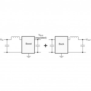
Figure 2. Cascaded boost and buck stages to create a buck-boost converter
SEPIC
The traditional approaches for single-stage, buck-boost conversion include SEPIC, ZETA or inverse SEPIC, and flyback. SEPIC is a common buck-boost topology for low- to medium-power levels. For wide-VIN applications it is suitable for up to 40W output power. It has only one switch and a diode and can use most boost controllers (Figure 3a). Higher switch voltages and currents (Figure 4) along with the presence of two windings degrade efficiency as power increases. With a DC-block capacitor and multiple inductors (or windings), the power stage and compensation design is tricky for non-experts.
The power level or efficiency can be boosted, if the rectifier diode is replaced by a synchronous MOSFET (Figure 3b). Still the combination of higher switching losses and high currents limit the output power well below 100W.
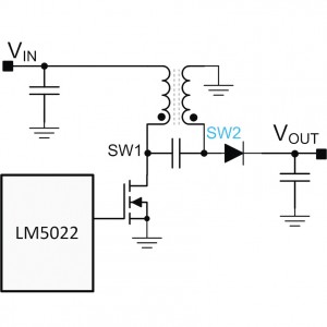
Figure 3A
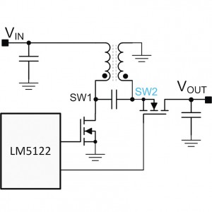
Figure 3B: SEPIC topology (inductors need not be coupled): a) non-sync SEPIC; b) synchronous SEPIC.
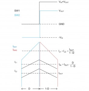
Figure 4: SEPIC waveforms.
Flyback
Flyback topology is often used for isolated DC/DC conversion. But it can be used as a non-isolated, non-inverting buck-boost (Figure 5a,b). This topology has discontinuous currents, both at the output and at the input. As a result, the RMS current is high in the two windings and switches.
Discontinuous currents in the windings (Figure 6) make it susceptible to leakage-induced spikes on the switch nodes. Snubbers are usually necessary to reduce the spikes to acceptable levels. The voltage ratings of switches and diodes are (VIN+VOUT) with additional margin added for leakage-induced spikes.
As in the case of SEPIC, synchronous designs can extend the power range (Figure 5b). Similar SEPIC designs can have higher efficiency than a flyback. This is because of lower RMS currents in the SEPIC inductor windings and extra losses caused by leakage in the flyback.
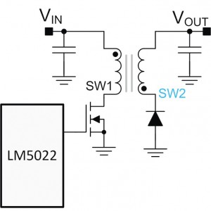
Figure 5a
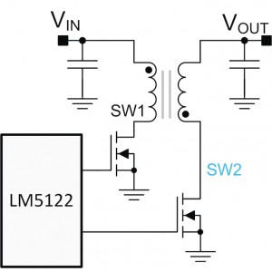
Figure 5: Flyback topology (usually needs snubbers, not shown): a) non-sync flyback; b) synchronous flyback.
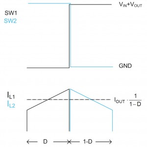
Figure 6. Flyback waveforms.
Single inductor two-switch buck-boost
The two-switch/two-diode single inductor buck-boost converter (Figure 7) enables the simplest non-inverting buck-boost design. The converter operates in buck-mode when VIN> VOUT. For VIN~VOUT and VIN<VOUT, the converter switches in buck-boost-mode (Figure 8) where both legs switch in every cycle.
Single inductor results in small solution sizes compared to SEPIC or flyback. The design is relatively simple. The FET ratings are reduced (from flyback or SEPIC case) to VIN on the input leg and VOUT on the output leg. Lower voltage stresses result in lower switching losses. Lower voltage FETs usually have better QG*RDSON, resulting in further reduction in losses.
Simple design notwithstanding, the two-switch, buck-boost has two diodes in series with the output for most of its operation. These losses in the diodes limit the output power to about 25W.
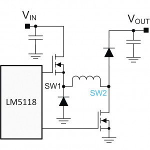
Figure 7. Two-switch, single inductor buck-boost.
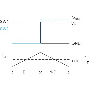
Figure 8. Two-switch, single inductor buck-boost waveforms in buck-boost-mode.
Four-switch, buck-boost
The four-switch, buck-boost topology (Figure 9) combines a single inductor design with synchronous rectification for both buck and boost legs. The operation is divided into three different modes. When VIN is close to VOUT, it operates in a buck-boost. When VIN is much higher or much lower than VOUT, it operates as a buck or as a boost converter. Boost-mode operation (Figure 10) has significantly lower switch and inductor currents than buck-boost operation, resulting in lower losses compared to other buck-boost topologies for low-input voltages.
Just as in a two-switch, buck-boost, the switch ratings are reduced to VIN on the input leg and VOUT on the output legs. Lower voltage stress on MOSFETs allows selection of lower voltage MOSFETs with better QG*RDSON characteristics. Better FETs and smaller voltage stresses on the FETs result in lower losses.
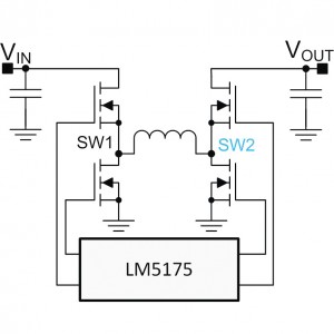
Figure 9. Four-switch, buck-boost.
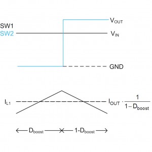
Figure 10. Four-switch, buck-boost waveforms in boost-mode.
Comparison of buck-boost topologies
A summary of voltage and current stresses in different buck-boost topologies is presented in Table 1. Items in red show that the topology has lower voltage or current stress and will likely result in lower losses and better efficiency. The inductor current ripple has been ignored. The results show the single inductor (LM5118 and LM5175) topologies have lower switch voltages and have lower switch currents for buck operation. The four-switch, buck-boost (LM5175) has lower switch and inductor current when boosting compared to all other solutions.
Another observation from this table is that SEPIC has lower inductor currents than flyback converter.

Table 1. Comparison of switch and inductor voltage/currents in buck-boost topologies
Note 1: Flyback assumed 1:1 turns ratio
Note 2: Inductor ripple ignored
Note 3: Flyback has current flowing in only one winding at a time.
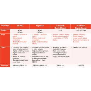
Table 2. Pros and cons of buck-boost topologies
Table 2 summarizes the pros and cons of the different buck-boost topologies.
Note: Power ratings in () are for synchronous SEPIC and flyback designs.
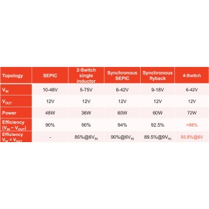
Table 3. Representative power and efficiency for buck-boost topologies.
Source: TI reference designs.
Table 3 shows a survey of reference designs developed for different topologies. The examples showcase the power level and efficiencies achievable in these topologies.
Selecting the right buck-boost topology
The designer has a range of topologies to choose from when creating a buck-boost converter. The SEPIC and flyback use multiple inductor or windings and can provide 40W for non-synchronous designs and 60W for synchronous designs with satisfactory results. The solution size tends to be larger because of multiple inductors or windings and the efficiency drops at higher power level. The two-switc,h buck-boost is a simple choice for low power levels that is easy to design and avoids the complications of multiple inductors or coupled inductors. The four-switch topology provides the most compact and efficient buck-boost solution for up to 250W.
References
- John Betten. Power supply topology: SEPIC vs flyback, Electronics Weekly
- John Betten. Benefits of a coupled-inductor SEPIC converter, TI analog Applications Journal, 2Q 2011
- Jeff Falin. Designing DC/DC converters based on SEPIC topology, TI analog Applications Journal, 4Q 2008
- Download these datasheets: LM5022, LM5122, LM5118, LM5175