Proper techniques critical to ensuring integrity of low current measurement applications
By Charles Cimino, marketing director, Keithley Instruments, a Tektronix Company
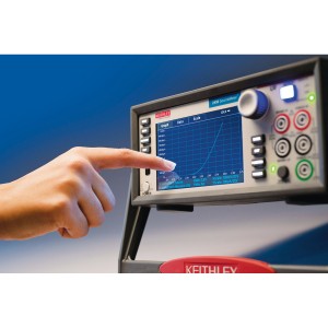
Test & Measurement EngineeringEnsuring the accuracy of low current measurements requires an understanding of both the advantages and limitations of the instrumentation used, as well as an awareness of sources of error that can limit their sensitivity. Source measure unit (SMU) instruments (Figure 1) are increasingly popular instrumentation options for these applications because they combine precision current and voltage sources with sensitive detection circuitry for sourcing and measuring current and voltage simultaneously. Their flexibility and ease of programming simplify using these instruments in both benchtop R&D configurations and automated test systems. (*See Figure 1)
Minimizing noise
An instrument’s current sensitivity is limited mainly by noise. The DUT also plays a part in the level of current a given instrument can detect because its source resistance (RS) establishes the level of Johnson current noise (IJ), the low-level noise caused by temperature effects on electrons in a conductor. Cryogenic cooling is sometimes used to reduce noise but adds cost and complexity. Although the noise bandwidth can be reduced by filtering, this slows the measurement significantly. Decreasing the DUT source resistance will also decrease the Johnson current noise, but this option is typically unfeasible.
Additional sources of current complicate low current measurements. For example, the coaxial cables used can generate as much as tens of nanoamps due to the triboelectric effect. This occurs when a cable is flexed and its outer shield rubs against its insulation; electrons stripped from the insulation are added to the current total. In applications such as nanotechnology and semiconductor research, the generated current may exceed the current to be measured from the DUT. To minimize the triboelectric effect, use low-noise cables with an inner insulator of polyethylene coated with graphite underneath the outer shield, minimize test cable lengths, isolate the test setup from vibration, and tape cables to a stable surface to prevent movement.
The piezoelectric effect, current generated by mechanical stress on susceptible materials, is another source of low current measurement error. Some commonly used materials, such as polytetrafluoroethylene (PTFE) dielectrics, can produce a relatively high current for a given amount of stress and vibration. To reduce piezoelectric effects, eliminate mechanical stress on insulators and choose insulating materials with minimal piezoelectric properties, such as ceramics.
Dielectric absorption, which occurs when a voltage across an insulator is high enough to cause positive and negative charges to polarize, can also degrade measurement accuracy. When the voltage is removed from the insulator, it gives up the separated charges as a decaying current, which is added to the total current measured. The time for the current to dissipate can range from minutes to hours. To minimize dielectric absorption effects, apply only low-level voltages to insulators used for low current measurements.
Contamination from salt, moisture, oil, excess solder, or even fingerprints on the surface of the insulator or a printed circuit board can also create problems. On an insulator, contamination can form a battery at a sensitive current node, generating nanoamp-level noise currents. To prevent contamination, wear gloves when handling insulators or simply avoid touching them. Minimize the use of solder and clean soldered areas with an appropriate solvent, such as isopropyl alcohol. Use a clean cotton swab for every cleaning, and never dip a used swab back into the solvent.
A magnetic field of changing intensity can cause current to flow in nearby conductors, as can the motion of a conductor within a magnetic field. To avoid false readings, shield the measuring instrument or system from magnetic fields.
Low current application examples
The following examples illustrate some especially challenging low current measurement applications, including measuring the photoconductive current of a PIN photodiode, Avalanche Photodiode Reverse Bias Current Measurements, and C-V characterization of carbon nanotube FETs.
Photoconductive current of PIN photodiode
A photodiode is a type of diode or photo detector that converts light into a current or voltage, depending on whether it is in the photovoltaic (zero-bias) or photoconductive (reverse-bias) mode. When the photodiode is in the reverse-bias mode, the output current is directly proportional to the light intensity applied to the photodiode junction. Consequently, photodiodes can be used to detect even very small quantities of light in a wide range of applications, including photography, light detectors, medical imaging instrumentation, and optical communications.
When the photodiode is reverse-biased, the resulting current is a combination of the photocurrent (obtained with light) and the dark current (no light). The photocurrent is typically constant as a function of the applied voltage. However, the dark current is a small leakage current induced by an applied voltage. The dark current is a thermally activated leakage of the PN junction; it is often measured as a function of temperature. The photocurrent and dark current measurements can be made with an SMU instrument that can sweep voltage and measure current over a wide range.
Figure 2 illustrates a low current, dual-channel SMU instrument connected to measure the photocurrent of a reverse-biased photodiode. The instrument used in this example is particularly suitable for this application because it can sweep the voltage and measure the current with <1fA resolution. It can also measure the forward bias I-V characteristics of the photodiode. When used for this purpose, the Kelvin (four-wire) method should be used to connect to the DUT to prevent unwanted voltage drops from affecting measurement accuracy. Figure 3 illustrates the results of measuring the reverse-bias current of a PIN silicon photodiode in this way. In this example, the I-V curves were generated at different low levels of light intensity (L1–L3).
(*See Figure 2 & 3)
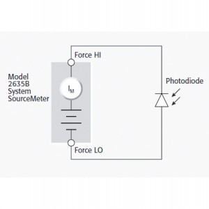
Figure 2
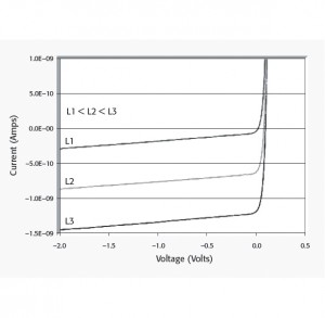
Figure 3
Avalanche photodiode reverse bias current measurements
An avalanche photodiode (APD) is a high sensitivity, high speed photodiode that has an internal gain mechanism activated by applying a reverse voltage. The gain of the APD can be controlled by the magnitude of the reverse bias voltage. A larger reverse bias voltage results in a larger gain. APDs are operated with an electric field strength such that an avalanche multiplication of photocurrent occurs similar to a chain reaction. APDs are used in a variety of applications requiring high sensitivity to light such as fiberoptic communications and scintillation detectors.
Common electrical measurements of APDs typically include the breakdown voltage, responsivity, and reversed bias current measurements. The maximum current rating for a typical APD is 10–4 to 10–2A, while the dark current can be as low as the 10–12 to 10–13A range. The maximum reverse bias voltage will vary, depending on the material of the APD, but can be up to 100V for indium gallium arsenide (InGaAs) APDs or up to 500V for silicon (Si) devices.
Measuring the reverse bias current of an APD requires an instrument that can measure current over a w
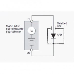
Figure 4
ide range, as well as output a voltage sweep. Instruments such as a combination picoammeter/voltage source or an ultra-sensitive SMU instrument are good options for meeting these test requirements.
Figure 4 illustrates a system configuration with an ultra-sensitive SMU instrument connected to a photodiode. The photodiode is placed in an electrically shielded dark box. To shield the sensitive current measurements from electrostatic interference, connect the box to the LO terminal of the instrument.
Figure 5 shows a current vs. reverse voltage sweep of an InGaAs APD that this instrument generates. Note the wide range of current measurements. The avalanche region becomes more pronounced with increasing light. The breakdown voltage will cause the current to flow freely because electron-hole pairs will form without the need for light striking the diode to generate current.
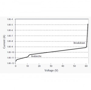
Figure 5
Current-Voltage Characterization of Carbon Nanotube (CNT) FETs
Carbon nanotube transistors (CNTs) have been the subject of much scientific research in recent years, due not only to their small size but their remarkable electronic and mechanical properties and wide range of potential applications. In particular, researchers are studying CNT-based devices, such as CNT FETs, for possible use in applications such as sensors, transistors, memory devices, etc. Characterizing the electrical properties of delicate nanoelectronic devices requires instruments and measurement techniques optimized for low power levels and high measurement sensitivity.
CNT FETs are three-terminal devices and require two or three SMU instruments for I-V characterization. Figure 6 (4-32) shows a typical test configuration for generating an IDVG curve. In this setup, two SMU instruments in a parameter analyzer are connected to the Gate and Drain terminals of a CNT FET. The Source terminal is either connected to a third
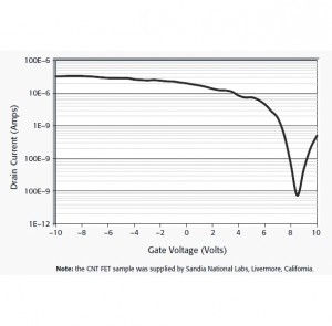
Figure 7
SMU instrument or to the Ground Unit. For the drain current vs. gate voltage test, SMU1 sweeps the gate voltage (VG) and SMU2 outputs a constant DC drain voltage (VD) and measures the resulting drain current (ID). This configuration allows obtaining a DC I-V drain family of curves easily by changing the function of SMU1 to step the gate voltage and SMU2 to sweep the drain voltage and measure the drain current.
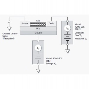
Figure 6
Figure 7 is an ID-VG plot of a CNT FET. In this curve, the drain voltage was set to a constant 2V. The SMU instruments with preamps in this system allow measuring current over a wide range from 100mA down to 100aA resolution.
To prevent damage to the device while performing I-V characterization, it’s important to limit the amount of current that can flow through the device, which can be done by adjusting the source limit (compliance) on the SMU instrument.
When measuring low current on CNT FETs, a variety of sources can generate noise, including particle collisions, defects, AC pickup, and electrostatic interference. Always use shielding techniques and the appropriate line cycle integration time to minimize noise.
Make sure the probes are in the up position (not in contact with the device) when connecting and disconnecting instruments from the terminals of the device. The process of moving cables has the potential to inject charge into the device and cause damage.