Enigma Interconnect makes bare pcbs with X-ray drilling, routing
Stephen Law
Electronics Production / Materials Contract Manufacturing Engineering Supply ChainToday’s demanding printed circuit board (pcb) design specifications require the latest technology advances for processing multi-layer panels – increasing the accuracy of all boards, according to John Parsons, engineering manager, Enigma Interconnect. By using x-ray drilling and routing, bare pcb manufacturers, such as the Burnaby BC-based board maker can detect and measure reference targets with ultra-fine accuracy.
“In fact, it is the best and only way to properly identify and correct displacements in the board pressing process,” says Parsons. “The ability to drill down to 0.004-in holes into pcbs as well as apply surface marks via CCD optical registration makes this equipment critical for achieving today’s pcb design requirements.”
Representing one of Western Canada’s largest manufacturers of high quality bare pcbs, Enigma Interconnect uses the Inspecta S HLP dual-station X-Ray drill machine from Pluritec.
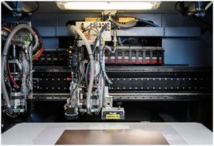
Enigma Interconnect’s Inspecta S HLP dual-station X-Ray drill machine from Pluritec.
“We are able to detect and measure reference targets with ultra-fine accuracy ideal for the latest Internet of Things (IoT) design innovations,” Parsons continues.
The Pluritec patented ‘One Step X Ray’ system can x-ray the pattern, perform the stretch/skew calculations and make drill and or rout process in one pass without any human intervention – leading to extremely high accuracy. The system also utilizes the CMM package so it can perform complex measurements and records for process statistical control.
“Any minor deviations in the geometry of the circuit board image compared to the geometry of the drill hole coordinates can now be identified,” says Parsons. The system targets the optimum drill reference point for each axis, with an optimal interpolation for all layers on multilayer boards.
By adopting x-ray drilling and routing, Enigma Interconnect can now resolve potential process problems with its bare pcbs before they occur – making this equipment critical for delivering specified pcb design requirements. Parsons says Enigma has also invested in technologies such as direct imaging and new solder mask processes to reduce its turnaround times and improve product quality, yields and to minimize process deviation.